|
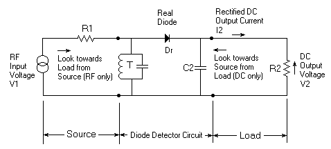
A New Diode Detector Equivalent Circuit, with a Discussion of the Linear-to-Square-Law Crossover Point: the signal level at which the detector is functioning midway between linear and square-law operationby Ben H. Tongue Quick Summary: The purpose of this article is to describe and and then compare a new diode detector equivalent circuit (DDEC) to a real world detector circuit (RWDDC), such as might be used in a crystal radio set. This equivalent circuit uses an ideal diode. Comparisons are made using SPICE simulations of the two circuits. Calculations using equations given in Article #15A are also supplied for comparison. The concept of the Linear-to-square-law crossover point (LSLCP) in the relation between output DC and input AC power is introduced (not to be confused with the exponential relationship of DC current to DC voltage in a diode). Part 1: General Description of a Diode Detector. The new diode detector equivalent circuit (DTEC) is based on the idea that a detector diode imbedded in a proper circuit can be thought of as a 'black box' device that converts RF power into DC power. Some power is lost in the process and that is called Diode detector insertion power loss (DDIPL). This approach completely avoids such concepts as duty cycle, pulse current, bypass capacitor charging and non-linear instantaneous voltage/current relationships. It is also consistent with the material given in Article #1. The peak-detector, capacitor-charging-current line of thought is good when signal levels are high enough to assure that true peak detection occurs. It is not very useful when signal levels are low. However, when all is said and done, the more different valid ways one can use in thinking about how a circuit works, the better becomes one's understanding of that circuit. This analysis applies to an AM detector fed by a CW RF sine wave voltage of frequency fo: It has a peak (not RMS) value equal to V1 and an internal source resistance of R1. The "maximum available RF input power" is called P1 (see section 2 in Article #0 for info on "maximum available power"). The DC output power delivered to the load resistor R2 is called P2. The DDIPL (in dB) is equal to ten times the log of the ratio between the two powers P2 and P1. This approach can also be used to model how a diode detector behaves with an AM modulated input signal by performing a SPICE simulation three times. Once with the RF signal equal to the value of the desired modulated wave's envelope minimum value, once with the signal equal to the carrier value and once with the signal equal to the crest value. The three DC output voltages give the minimum, carrier equivalent and peak value of the demodulated output audio wave. ***** Please do not skip this next paragraph! ***** To understand the new diode detector equivalent circuit, one must abandon the usual way of thinking the about the diode in a detector. Instead, one must think about the "diode detector circuit". This circuit includes a tank circuit T, the output capacitor C, as well as the diode. The shunt input reactance of the circuit is assumed to be zero at all frequencies except fo, the frequency to which the tank is tuned. The input resistance at fo will be discussed later. The output reactance of the circuit is assumed to be zero at all RF frequencies. The output resistance will be discussed later. A real world diode is a two terminal device. The "real world diode detector circuit" will be modeled as a "two port, four terminal device" having a pair of terminals for the input and another for the output. One of the input terminals is the "hot" input terminal; the other is "low". One output terminal is the "hot" one, the other is "low". The two "low" terminals are connected together and usually to ground. Please note, that in the topology of the two schematics shown below, the "Diode Detector Circuit" and the "Diode Detector Equivalent Circuit" both include the tank T and the bypass capacitor C2 as an integral part of the detector. Also, look at the circuits in this way: The tank circuit, looking towards the output, sees the diode as a one-end-grounded shunt load since the output bypass cap is a short at RF. The output load resistor, looking back towards the input, sees the diode as a one-end-grounded shunt DC resistive source since the input side of the diode is shorted to ground by the tank. See Fig 1. The detector tank circuit T is modeled as lossless and resonant to the input frequency fo. Losses in a real world tank can be accounted for by using Thevenin's Theorem to calculate the appropriate changes in V1 and R1. This leaves the circuit topology unchanged. See Article #1 for more on this subject. The value of the tuning capacitor in T is sufficiently large so that essentially no harmonics of fo can appear across T. This assures that the "pendulum-like resonator effect" of a high Q circuit will be available to supply the narrow, high-current pulses the diode requires every cycle when strong signals are handled. Another advantage is that tank-voltage-waveform peak clipping by diode conduction is essentially prevented when the current pulses are drawn. All this assures that the input impedance to the detector will be linear over one cycle of RF and the input current to, and voltage across the tank T will always be sinusoidal, no matter how weak or strong the input signal. See Article #8 for an illustration of typical waveforms. A reactance value for the tank capacitor equal to less than one hundredth of the value of R1 will be sufficient. The DC resistance of the tank inductor should be small enough so that no appreciable DC voltage will appear across it. A value less than one hundredth of the value of R2 will be sufficiently small. This assures that all of the output DC power goes into R2. The bypass capacitor C2 has a very low reactance compared to the load resistor R2 at the frequency fo. Since C2 acts as a short circuit across R2 at the frequency fo, all of the RF voltage across T will appear across the Diode. The time constant, R2*C2 should be long compared to the time for one cycle of fo. Part 2a: Discussion of the new Diode Detector Equivalent Circuit.
To gain an understanding of the Diode Detector Equivalent
Circuit (DDEC), first consider the following line of thought:
See Fig. 1. Let the input RF voltage V1 become very low.
V1, at a frequency fo, looking toward the load resistance R2, will see
an RF resistance (at fo) equal to the junction resistance of the diode
at zero bias. At this very low signal condition the detector input
resistance is not affected by any changes made to R2. The value
of this junction resistance is the slope of the diode V/I curve at the
origin. From a differentiation of the ideal diode equation, the numerical
value of this resistance is: (0.0256789*n)/Is ohms at a temperature
of 25 degrees C. Let's call this Ro. Is and n are parameters
in the ideal diode equation. (For a discussion of Is, n, etc., see the
text after the schematics in Part #1 of Article #1). From the
load resistance R2, looking back toward the input, one sees the same
resistance value Ro, and it is independent of any changes at the source.
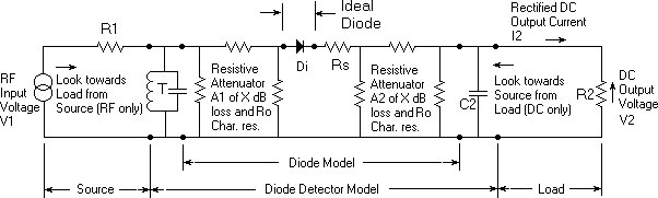
Now look at Fig. 2. Here, the real world diode has been changed
to a theoretical ideal diode and two attenuators, A1 and A2, of characteristic
resistance Ro have been are added. If V1 becomes zero, the attenuators
A1 and A2 must be set to infinite attenuation to enable the model to
duplicate the behavior of the circuit in Fig.1. When an input
signal is applied, the values of A1 and A2 must become finite.
The DDIPL is equal to the sum of the loss of each attenuator plus the
impedance interface loss between the ideal diode Di and each attenuator,
as well as any mismatch loss between R1 and the detector as well as
between R2 and the detector (See ** after Table 2). SPICE simulation
shows that the diode detector equivalent circuit does a pretty good
job modeling the operation of a real world diode detector. To
verify this, one can perform a SPICE simulation of Fig.1 and Fig. 2
with V1, R1 and R2 the same in each case. The attenuation value
of A1=A2 dB must be set to a value that causes the output, V2, in Fig.
2 to be the same as in Fig.1. The input impedance match of the
two simulations differ from each other by less than 14% over an input
power range of 48 dB, centered at the Linear-Square-Law Transition
(LSLCP) point. This is the main area where the results from
the DDEC simulation differ from those of the RWDD. The input resistance
of the DDEC is always higher than that of the REDD. This equivalent
circuit seems to work for signals from well below the LSLTP point
up to levels just before "Diode Reverse Breakdown Current" comes into
the picture.
Fig. 2 Some definitions and conditions that apply to Fig. 2 follow:
Table 1 shows three groups of data: SPICE simulations of the RWDDC and the DDEC, and a set of calculated values from equations appearing in Article #15A. Data is shown for three input power levels for each data group The levels are: 1) The input power that will operate the RWDDC at its LSLCP [Plsc(i)], 2) 1/128 the value of Plsc(i), and 3) 128 times the value of Plsc(i). These power levels are believed to be correct if the input and output impedances of the detectors are impedance matched, using appropriate values for R1 and R2. Actually, in the simulations, R1=R2=Ro=0.0256789*n/Is. This causes the required input power for the desired output to be somewhat greater than if input and output were perfectly matched. The attenuators A1 and A2 in the DTEC are set equal to each other, and to a value that causes the output power of the DDEC to closely equal that of the RWDDC. SPICE parameters for the diode in the RWDDC and "Calculated values" are: (Is)=38 nA and n=1.0*. The "calculated values" assume impedance matched conditions. The SPICE circuit simulation program "ICAP/4" from Intusoft was used in all simulations.
* The n of real world diodes is never 1.0. Actual values of good detector diodes are usually between 1.03 and 1.10. The input and output power values given in the data group for the RWDD can be corrected if n is over 1.0 by adding 10*log (n) dB to the P1 and P2 figures. Keep in mind that n and (Is) are most always independent of current for Schottky diodes. This is not the case for silicon pn junction or germanium point contact diodes. A New diode detector equivalent circuit, with a discure law crossover point. *** Calculations for a RWDDC using equations #6 and *2an given in Article #15A. These equations assume perfect impedance matching at the input and output. Part 2b: An alternative DDEC. An alternative 'diode detector equivalent circuit' (DDEC2) can be formed by moving the tank circuit T from its position shown in Fig. 2 to the left hand terminal of diode Di and moving the bypass capacitor C2 to the right hand end of resistor Rs. This equivalent circuit always operates as a peak detector, so no 'excess loss' need be accounted for. The loss for attenuators A1=A2, at any input signal level may be calculated from equations #3n and #6 in Article #15A. Loss for A1=A2=5*log(DIPL from equation #3n) dB. The input impedance (S11) of the DDEC2 approaches that of the RWDD at high and low input power levels. Its input resistance at intermediate power levels is always lower than that of the RWDD. Part 3: Further Discussion of the Linear-to-Square-law Crossover Point. The RF input resistances in the simulations of the DDEC (Fig.2) are within 17%, 17% and 8% at the low, medium and high power inputs respectively, of the simulated resistances of the RWDC (Fig 1). The DDIPL values at each input power level for the circuits in Figs. 1 and 2 were set to within 0.1 dB of each other by adjustment of the loss in A1 and A2. Operation at the LSLCP: Operation at the LSLCP can be said to occur when the detector is operating half way between its linear and square law response mode, the point where the two areas overlap equally. At this point there is a sqrt(2) dB change in output power for every 1.0 dB change in input power. Operation at power levels below the LSLCP point: As input power levels are lowered, the DDIPL approaches 10*log{[I2/(I2 + Is)]}-6 dB. Operation at power levels above the LSLCT point: Here, the DDIPL tends to approach zero, but the detector input and output impedance match starts to deteriorate. This is the regime where the mode of detection changes from "averaging" to "peak". (See Article #0, Section 5 for an explanation of this effect.) Re-matching the input and output circuits at these higher input RF power levels recovers the excess loss caused by the mismatch, and results in the performance given by the equations in Article #15A. Input/Output impedance interaction: When an input signal is present, interaction between the input and output circuit occurs. That is because the attenuation of the attenuators A1 and A2 must become finite and that lets the interaction come through. If the output load R2 is reduced, the input resistance to the detector will be reduced. If the input source resistance R1 is reduced, the output resistance of the detector will be reduced. This interaction is dependent on the strength of the input signal. For greater input signals, there will be less DDIPL (Lower values for attenuators A1 and A2) and greater interaction. If DDIPL approaches zero, the output resistance will approach two times the source resistance R1. Similarly, the input resistance will approach 1/2 the load resistance R2. If the input signal power is reduced, detector input and output resistance values become decoupled from each other and both approach Ro. See the paragraph below Fig. 1. Overview: One can think of a diode detector circuit as a device to change input RF power to an almost equal amount of DC output power, provided the input power level itself is high enough. In this instance the attenuators A1 and A2 in Fig. 2 have very low values. If the input power is reduced, A1 and A2 increase in loss, thus reducing the output power. At low input power levels, square law operation occurs. In this region, if the input power is reduced by, say, 1 dB, the loss in attenuators A1 and A2 are each increased resulting in an output reduced by 0.5 dB. Voila, square law operation! There is an extra loss besides that of A1 and A2. It is the interface mismatch loss between each attenuator and the diode Di as well as input and output mismatch losses. This interface loss varies as a function of input power. It is about zero when the values of A1 and A2 are very low (large signal power condition) and approaches 3 dB for each attenuator at low signal power levels (total of about 6 dB). See the Table 1 above and the ** comment below it. #10 Published: 04/04/00; Revised: 10/27/2002 |