|
Quantitative insights into Diode Detector Operation derived from Simulation in SPICE, and some Interesting new Equations relating diode parameters to weak signal sensitivityBy Ben H. Tongue
This Article, #15A, used to be Part 1 of the old Article #17. Definitions of terms to be used:
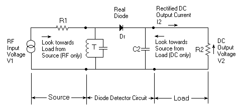
The diode detector circuit to which we will refer is shown in Fig. 1.
Assumptions used in the following discussion:
Approach: The RF signal input power range is divided into two regions and one point; impedance and power relationships are determined. Refer to Figs. 2 and 3. Two Cases will be considered. In Case A, R1=R2=Rx=0.0256789*n/Is. In Case B, R1=Rx/sqrt2 and R2=Rx*sqrt2.
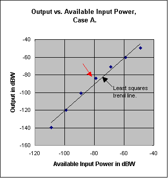
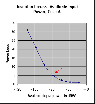
Transition from the linear to the square law region: All good diode detectors, at high input power levels, if well impedance matched at input and output, have a low insertion power loss (a fraction of a dB). If the input power is reduced, at first the output will drop approximately dB for dB in step with the input. If the input is further reduced, the output will start to drop faster (in dB). This can be thought of as the onset of noticeable 'detector insertion power loss'. The insertion power loss at the LSLCP, in two SPICE simulations (see Cases A and B below), is about 5 dB. Put another way, at the LSLCP the output power is about 0.3 times the available input power. This power loss figure changes by less than 0.1 dB between Cases A and B. Most crystal radio sets can deliver a readable signal at an input of Plsc(i) Watts. It would obviously be desirable to lower the input power at which the LSLCP occurs so that more of the weak signals would be closer to the linear mode of operation, experience less insertion power loss and therefore be louder. Example SPICE simulation of a diode detector at 25° C.: Figs. 2 and 3 show power relations at various power levels. The LSLCP is shown by a red arrow. In the SPICE simulations for these graphs, the source and load resistances, R1 and R2, are equal to Rx (Case A). The DIPL values for Case B (Fig.3) are within 0.4 dB of those of Case A. The main difference is the lower DIPL values in Case B at high input powers. For instance, the insertion power loss at an input of -48.912 dBW is 0.76 dB for Case A and 0.30 for Case B. The loss figures from the equations that follow are quite close to those that occur in a SPICE simulation of both Case A and Case B. At input power levels several times or more below the LSLCP, the impedances of the input and output ports of the detector both approach Rx for both Cases, A and B. At input power levels several times or more above the LSLCP, the detector approaches operation as a peak detector having a low insertion power loss. In this condition the input RF resistance of the detector approaches half the output load resistance and the output resistance of the detector approaches twice the RF source resistance. Summary: In Case A, the detector input and output ports both approach an impedance matched condition when the signal power is several times lower than that at the LSLCP. At signal power inputs several times greater than that at the LSLCP, a moderate impedance mismatch exists at both the input and output ports. In Case B, conversely, the detector input and output ports are both are moderately impedance mismatched when the signal power is several times lower than that at the LSLCP. At signal power inputs several times greater than that at the LSLCP, both input and output ports approach an impedance matched condition.
Note the following in Fig. 2: At input power levels well above the LSLCP, the relationship between input and output power (see the data points, not the Least Squares Line) approaches linearity. That is, the output changes about one dB for every one dB change in input. At input power levels well below the LSLCP, the relationship between input and output power (see the data points, not the Least Squares Line) approaches a square law relationship. That is, the output power changes about two dB for every one dB change in input power. This has bad implications for weak signal reception. If a weak signal fades, the detected signal will drop twice as many dB as the reduction in input signal strength. For best weak signal sensitivity, one should push the LSLCP to as low a power level as possible. This moves weak signals closer to the LSLCP and linear operation (less detector power loss), and thus increases volume. Lowering of the LSLCP power is associated with using a diode having low values for n and Is, and impedance matching the antenna-ground system impedance and headphone impedance to the now higher values of detector input and output impedances. For good results, one must make sure the impedance transforming means does not introduce other losses. A high Q tank inductor, tuning capacitor, and low loss audio transformer are important. It may be difficult to achieve the required greater impedance transformations in a low loss manner. Example: Assume that Is=38 nA and n=1.03, as was used in the graphs and chart above. Rx becomes approximately 696009 ohms. R1 and R2 are each fixed at 696009 ohms for all simulation points in Case A. This establishes a very good input and output impedance match at low signal levels and a moderate match at higher levels. The input return loss (S11) is better than -14 dB at signal levels up to 12 dB above Plsc(i). S11 approaches about -9.5 dB at very high input power levels. The input impedance match conditions are reversed in Case B. Rx is still 696009 ohms but R1 is set to 492153 and R2 to 984305 ohms. Now, at low input power levels, the input and output are somewhat mismatched (S11=-15.3 dB), but at high signal power levels, a very good impedance match is approached. The bottom row shows these two conditions. Unpublished information from Xavier Le Polozec indicates that the optimum practical compromise values for R1 and R2, for input powers well below the LSLCP to well above it is: R1=Rx and R2=Rx*sqrt2. The diode detector equations: The following equations are developed for the Class A termination condition of R1=R2=Rx. They give insertion power loss values to within a fraction of a dB of those provided by SPICE simulation for both Cases A and B. The output current, I2, is different for Class A and B. Observation of a curve of output vs. input power (in dB), from SPICE simulation of a Class A terminated detector reveals a slope of 1.5 at an input power value of -78.91 dBW, for the particular diode used. This is the LSLCP for input power. Another observation is that the rectified diode current I2 at the LSLCP point appears to be very closely two times the Is of the diode. This two times figure appears to be apply to all diodes. Note: The Plsc(i) of -78.91 dBW occurs when the detector parameters are R1=R2=Rx and the diode parameters are: Is=38 nA, n=1.03 and temperature is 25° C. In general, the 'two times' figure does not hold for termination conditions other than R1=R2=Rx. Calculation of diode detector output power when it is operating at its LSLCP: Differentiating the Shockley diode equation with respect to the diode junction voltage yields: Diode junction resistance=Rx=0.0256789*n/Is ohms. (0) At the LSLCP, I2=2*Is. (From the paragraph above) (1) Some obvious relations: Output power=Po=(I2^2)*R2 Watts. The output load R2 has been specified as equal to Rx, Rx is defined in equation (0). I2 is 2 times Is at the LSLCP (See equation 1). Substituting into the equation for Output power Po, we get, for the output power at the LSLCP: Calculation of the diode detector DC output voltage [V2lsc(o)] when it is operating at its LSLCP: Some simple manipulation of equations (0) and (2) results in the relation: V2lsc(o)=0.051*n Volts (2a) Calculation of the ratio of output power to input power (DIPLR) at any power level: A proper relation between Po, Pi and I2 obviously requires that I2 approach zero as Po/Pi approaches zero, that Po/Pi approach proportionality to I2 as I2 becomes low (the square law relation) and that Po approach Pi as I2 becomes very high. Also, at an output power of Plsc(o), I2 must equal 2*Is, as stated earlier. Curve fitting suggests this relationship: Po/Pi=(I2/(I2+4*Is)=DIPLR (3) Interesting note: Since, at the LSLCP, I2=2*Is (eq. 1), Plsc(i)=Plsc(o)*3. (4) Calculation of the diode detector input power when it is operating at its LSLCP: Substituting the value of Plsc(o) from equation 2 into equation 4 results in: Plsc(i)=0.308148*Is*n for the input power at the LSLCP (4a) Various relationships between input power, output power and diode parameters: A lot of mathematical manipulation of the relations given above results an equation that fits the simulation data quite well over the whole range of the graph in Fig. 2. Po=[sqrt(0.102716*n*Is+Pi)-sqrt(0.102716*n*Is)]^2 Watts. (5) Po={sqrt[Plsc(o)+Pi]-sqrt[Plsc(o)]}^2 Watts. Normalized to Plsc(o). (5n) A rearrangement of the terms in equation (5) yields: Pi=Po+sqrt(0.41104*n*Is*Po) Watts. (5r) Pi=Po+2*sqrt(Plsc(o)*Po) Watts. Equation (5r) normalized to Plsc(o), by using equation (2). (5rn) From equation (5r), at low output power power levels, the input power required to produce a given output approaches: Pi=sqrt(0.41104*n*Is*Po) (5Li) Prearranging terms of equation 5Li: Po=(Pi^2)/(0.41104*n*Is) (5Lo) An equation that fits the detector Insertion Power Loss Ratio (DIPLR) is obtained by dividing equation (5) by Pi: DIPLR=[sqrt(1+0.102716*n*Is/Pi)-sqrt(0.102716*n*Is/Pi)]^2 (6) DIPLR={sqrt[1+Plsc(o)/Pi]-sqrt[Plsc(o)/Pi]}^2 Normalized to Plsc(o) by dividing right side of eq. (5n) by Pi (6n) The Insertion power loss (DIPLR) at which a diode detector is operating can be determined by noting the DC rectified output voltage: Adjust the DC component of the diode load to equal its axis-crossing resistance (0.0256789*n/Is ohms).** Measure the DC voltage V2 developed across the DC load. Some simple manipulation of equation (3) above results in equation (7). DIPLR=V2/(V2+0.1027156*n) (7) ** See articles #16 and #27 for info on determining the Is and n of diodes as well as measurements on some diodes. Equation (5r) seems important. It shows that the input power required for a specific output power is reduced if n and/or Is is reduced. At low input powers, the required input power for a specific output power approaches direct proportionality to the square root of n and/or Is, as shown in equation (5Li). The product n*Is can be considered to be a 'figure of merit' for diodes as weak signal detectors, provided input and output impedance matching exist and losses from passive components remain unchanged. The ideality factor (n) and saturation current (Is) of the diode are important parameters in determining ultimate very weak signal sensitivity. If all other diode parameters are kept the same, the weak signal input and output resistances of a diode detector are directly proportional to n and inversely proportional to Is. Assume a diode with a value of n equal to oldn is replaced with an identical diode, except that it has an n of newn, and the input and output impedances are re-matched (the new impedances are doubled). The result will be a detector insertion power loss change of: 10*log(oldn/newn) dB. That is, a doubling of n will result in a 3 dB increase in insertion power loss, assuming the input power is kept the same and input and output impedances are re-matched. The result is a 3 dB reduction of output power (volume). A similar effect occurs if Is of the diode is increased except that this change reduces the impedances that must be re-matched instead of increasing them. Interesting note: A simple manipulation of Equations #0, 2 and 4 shows that, at the LSLCP, the RMS value of the AC signal at the input to the diode is: (0.08895*n) Volts, and it is independent of Is. One final equation: One can combine two equations: Rx=0.0256789*n/Is, as given in the "Definition of Terms" at the beginning of this Article and equation (5Lo) to come out with a very useful result relative to actual crystal set design. For a given input power, equation (8) gives the output power as a function of the diode axis-crossing resistance and ideality factor (for weak signals and matched conditions). Po={(Pi/n)^2}*(Rx/0.010554) (8) Let us review the conditions that apply to equation (8) before discussing it. 1) The signal power to the detector diode is well below the LSLCP (weak-signal reception). 2) Detector source and load impedances are well matched to Rx, the axis-crossing resistance of the diode (see "Definition of Terms"). Equation (8) indicates that the maximization of output power, when receiving weak signals, requires using a diode of low n because output power is shown to be inversely proportional to the square of n. Also, with other factors being fixed, higher source and load impedances increase output power in direct proportion to their increase in value (remember they are both kept equal to Rx). A real-world problem occurs when one manipulates the RF input and audio output impedance transformations when attempting to optimize them to get greater weak-signal volume. Their internal power losses can change and this is not accounted for in equation (8). The RF input impedance transformation loss probably won't change a lot if the ratio of unloaded to loaded Q of the tank doesn't change, and will not be treated here. Audio transformer loss is worth investigating. An audio transformer usually has a Manufacturer-stated loss that applies when it is used between the Manufacturer-stated impedances. When used between other impedances (higher, in the usual case with crystal sets), transformer loss will most always be greater. Equation 8 shows that the transformer winding connected to the audio output side of the diode detector should present the highest impedance possible but, then that is done, transformer power loss usually increases. A compromise is needed.
Warning: Don't use two diodes in series if you want the best weak signal sensitivity. The result of using two identical diodes in series is the emulation of an equivalent single diode having the same Is but an n of twice that of one original diode. Experimental measurements on eleven different diodes used as detectors is shown in Article #27. Close correlation between these equations and actual measurements is demonstrated. #15A Published: 04/10/2001; Revised: 12/07/2008 |