|
Get 3 dB more Output for Greater Volume on Strong Stations plus...By Ben H. Tongue
One third the total power in a 100% modulated AM signal is in
the sidebands that carry the audio modulation. An ideal, 100%
efficient Crystal radio set will convert all of the received sideband power to
audio output power. Call it audio power output #1. What about
the other two thirds of the power? That is the power in the
AM
carrier that carries no audio information but has twice the power of
the sidebands (at 100% modulation). This Article shows the circuit
of a device that can be used to extract that carrier power and use it to
operate a micro-power op-amp. The op-amp uses the detected audio voltage
from the diode detector for its input and provides an additional source
of audio power. Call it audio power output #2. These two audio power
sources, #1 and #2 can be added together to create a final output at least
3 dB more than the normally available audio power output #1.
1. Background Within the last year or so, Burr-Brown (now owned by Texas Instruments)
came out with a micro-power op-amp (OPA349) specified to work with as little
as a 1.8 volt DC power source. It draws a minuscule 1 uA quiescent
supply current. This op-amp opens the possibility of building a device
I call a "Free 3 dB Detector Load" (F3dBDL). I have found
that the F3dBDL will actually operate with an input signal low enough to
generate a rectified voltage as low as 1.2 volts DC. Maybe all the
OPA349s will work in this circuit at 1.2 volts. My F3dBDL requires
a minimum input carrier power of -53 dBW and a rectified DC voltage
of at least 1.2 volts.
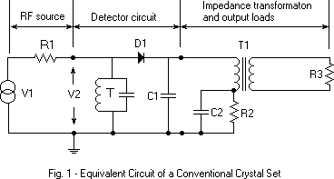
2. A conventional diode detector with standard output loads (DC and audio) Any crystal radio set that uses an audio output transformer can be represented
by the simple circuit shown in Fig. 1. V1, R1 represent the antenna-ground
power source, impedance transformed to the tank circuit. The detected
carrier power is dissipated in the resistive load R2. The detected
side-band power is delivered to the audio load R3.
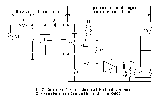
3. Conventional crystal radio set detector with the F3dBDL The F3dBDL is intended to be used with signals strong enough to cause
the detector to operate in its peak-detection mode. In this case,
the DC load R2, seen by the diode D1 should equal to two times the RF source
resistance R1. D1 should also see an AC load resistance of two times
R1, at the primary of transformer T1. (See Article #0 , Section 4,
for more info on this.) The power dissipated in the DC load R2 in
the circuit in Fig. 1 will be used, in Fig. 2, to power the op-amp U1.
In Fig, 1 the audio output power is delivered to the output load R3.
In Fig. 2 audio output power is delivered to two loads of value R3 and
k*(R3). With proper selection of the relative impedance transformation
ratios of T1 and T2, the value of k may be made equal to about 1.
In addition, the output currents of T1 and T2 become about equal.
In this case, no current will flow in connection X, and it can be eliminated.
This gives us one 600 ohm instead of two 300 ohm outputs.
The resultant load resistance of twice R3 will absorb twice the audio power
than did R3 in Fig. 1, although at twice the impedance (600 ohms).
The resistive network R4, R5, R6 and R7 biases + input terminal of U1 at
1/2 the DC supply voltage appearing across C2 and attenuates the detected
audio voltage appearing across C1 so that it will not overload U1.
The value of capacitor C2 is made quite large to enable it to hold steady
the voltage it supplies U1, between bursts of speech.
If all the power in the carrier could be changed to audio power and added to the main detector audio output, the total audio power would be tripled, a 4.8 dB increase. It would be nice if the op-amp had 100% efficiency in converting its input DC power to output audio power, but it doesn't. An ideal class B amplifier has a theoretical efficiency of 78.5%. Therefore, we lose at least 21.5% (1.05 dB) right off the bat. Other losses in the op-amp, the 1 uA quiescent current of the U1 and the bias network R5, R6 and R7 use up some more of the 4.8 dB. The transformer T1 has losses and uses up some more of the 4.3 dB. We are left with an output power from the U1, T2 combination about equal to that of a conventional crystal radio set. The two added together gives the 3 dB increase. There are some limitations in using the F3dBDL. The IC is specified to operate over a supply voltage range of 1.8 to 5.5 volts. In this circuit it seems to work well over a supply voltage range of 1.2 to greater than 5.5 volts. This corresponds to an input carrier power range of -53 to >-40 dBW. I have found, that for me, the volume to be too great for headphone use but barely adequate for high efficiency horn speaker use. If more than -40 dBW of AM signal carrier power is available, the F3dBDL can be made to handle it (and give a greater sound volume) if the F3dBDL is operated at a lower output impedance level. In this case, transformers T1 and T2 might have to be changed to ones with a lower transformation ratio. The impedance at the + signal input terminal of U1 is very high. Use care to minimize stray capacitance to ground at this point. Too much will roll off the highs. The high audio frequency output capability of U1 falls as signal strength and, as a result, supply voltage increases. This can cause audio distortion. The F3dBDL can also be used to increase the volume on weak stations. This is done by connecting a ceramic electric double layer high capacitance capacitor across C2, charging it up overnight on a strong station and then switching it to power the opamp for weak station listening later on. A 0.047 Farad capacitor will hold its charge for many hours in this application. One manufacturer of this type capacitor is Panasonic, and one of their distributors is Digi-Key Corp. If the load on the F3dBDL is a SP headphone set with the elements wired in series, bass response can be improved with a small subjective increase in volume. Consider the two headphone elements as the two impedance equal loads R3 and k*(R3), in Fig. 2. Restore the connection X. The element k*(R3) will have a much better bass response than the other one because it is driven by the low output resistance of the opamp. See "It is interesting to note" at the end of Section 1 in Article #2 for more info on this. Last, but not least, one should not expect too much from the F3dBDL. After all, a 3 dB or so increase in volume will not be perceived as a lot. The challenge of this project was to devise a way to use all of the power in an AM modulated signal, I believe that has been accomplished. #18 Published: 07/09/01; Revised: 04/06/2007 |