|
A New Way to look at Crystal Radio Design. Get Greater Sensitivity to very Weak Signals, and Greater Volume, less Audio Distortion and Improved Selectivity on Strong Signals
1. THEORY A crystal radio may be thought of as the cascaded connection of several basic components.
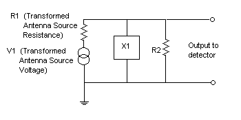
The Antenna and RF Tuned Circuit will be combined into three components. V1 and R1 represent the antenna induced voltage and resistance, impedance transformed by the tuned circuits and antenna reactance to the series-connected values seen by the diode detector. X1 represents the reactance of the tuned circuit(s) seen at its output terminals. Its impedance is considered to be substantially zero at harmonics of the frequency to which it is tuned. Its impedance is also substantially zero at DC and at Audio frequencies. R2 represents all the losses in the tuned circuits at resonance, as seen by the diode. This is not the conventional way of viewing the signal source for a detector.
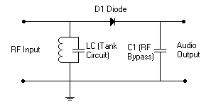
The Detector will be represented as follows: The LC tank assures that the input is effectively shorted to ground at DC and at audio frequencies as well as all RF frequencies except that to which it is tuned. The output is effectively shorted to ground at RF by C1.
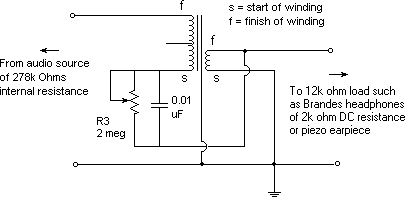
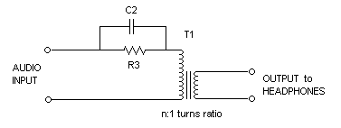
The Output Transformer circuit will be represented as shown below. The purpose of R3 and C2 will be covered later.
We start out with the assumption of no losses in the tuned circuits. This condition makes R2 equal to infinity, not a practical assumption of course, but it will simplify what follows. The input circuit then reduces to a simple series connection of the parallel tuned circuit, impedance transformed antenna voltage, and a series resistance. This resistance includes the effects of radiation, antenna, lead-in and ground circuit resistance. A simple transformation enables us to eliminate R2 entirely by combining its effects into a changed value for R1 and a new value for V1. The new value for V1 is: V1new = V1old*(R2old/(R1old + R2old)). The new value for R1 is: R1new = (R1old*R2old)/(R1old + R2old). With this transformation the new value for R2 is infinity, so it can be eliminated from the circuit. Of course, the maximum available power from the new source 'V1new, R1new' is less than what was available from the original source 'V1old, R1old' by the amount that was dissipated in R2. From now on, V1new and R1new will be referred to as V1 and R1. The RF Source Voltage (V1) is assumed to be un modulated CW. The transformed V1 (RMS) and R1 represent a Power Source of available power Pa = (V1^2)/(4*R1). This is the most power it can deliver to a load. It is also sometimes called the "Incident Power". For the load to absorb this power, the load itself must equal R1, and then it is called an 'Impedance Matched Load'. Changing the impedance transformation in the tuned circuit(s) changes the values of V1 and R1. This does not change the available power. That is still (V1^2)/(4*R1). As an illustration, if V1 is doubled, R1 must quadruple thus keeping the power the same. The approach we will use in this analysis is to minimize impedance mismatch power loss between the transformed antenna resistance and the diode detector input RF resistance as well as between the detector audio output resistance and the headphones. We will show that the diode detector power Loss (DDPL), for very weak signal levels, can be minimized by using a diode with as low a Saturation Current (Is) as possible if all else is equal. In addition, the lower the ideality factor (n) of the diode, the greater will be the sensitivity to weak signals. The limitation here is that if a diode with a lower Is used, the required diode RF source and audio load resistances go up in value. That limit is reached when the diode is connected to the top (the highest impedance point) of the tuned circuit. The high frequency audio cutoff point may be reduced because of unavoidable winding capacitance in the audio output transformer acting against the required higher transformed headphone effective impedance. The most important diode parameters to consider for Xtal radio operation are saturation current 'Is' and 'n'. They show up in the Shockley diode equation: Id = Is*(exp((Vd-Id*Rs)/(0.026*n)) -1), at room temperature. In crystal radio applications, the Id*Rs term may be neglected because it is usually much smaller than V. The equation then becomes: Id=Is*(exp(Vd/(0.026*n))-1). (1) This equation provides a good approximation of the V/I relationship
for most diodes, provided the parameters Is, n, and Rs are really constant.
Some diodes, especially germanium and silicon junction diodes seem to
have Is and n values which increase at very high currents (higher than
those usually encountered in crystal radio operation). In some of
these diodes, the values of Is and n also increase at very low currents,
harming weak signal reception. Is and n are usually constant in
Silicon Schottky diodes, over the current range encountered in crystal
radio use.
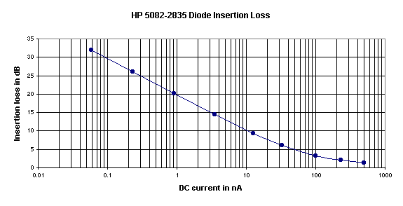
Agilent specifies the values of Is, Rs and n for Schottky diodes in their catalog. They are listed in the table of SPICE parameters. To find some SPICE parameters for other diodes (germanium types etc.), one can use used a neat Computer Program written by Ray Waugh of Agilent. To use it one measures the diode forward voltage at five different currents (0.1 mA, 1.0 mA, 4.8 mA, 5.0 mA and 5.2 mA). Ray&39;s program runs on Mathcad 6.0 or higher. One enters the five voltages and voila, out come Is, n, and Rs. Remember this caveat: The program assumes that Is, n and Rs are constant and do not vary with diode current. If they do vary, one can change the first two currents (0.1 and 1.0 mA) to cover a smaller range, say, two-to-one, that bracket a desired diode operating current and get the Is and n values for that current. Ray told me that if anyone wants a copy of this program, it would be OK for me to supply it. A simplified method of approximating Is (n must be estimated) that does not require having Mathcad is described in article #4. A complete description of a test set-up and calculation method for determining both n and Is is shown in Article #16. Here is what I have found experimentally through a SPICE simulation of a diode detector. If a detector diode is fed by an RF source resistance of n*0.026/Is ohms and is loaded by an audio load resistance of n*0.026/Is, then both input and output ports are matched with a return loss of better than 18 dB, assuming the signal is of weak to medium strength. This satisfies the condition of very low mismatch but only holds true for diode rectified currents of up to about 5*Is. An impedance matched diode detector insertion loss at a rectified current of 5*Is is about 3-4 dB. The input and output impedance match starts deteriorating with a DC rectified current of over about 5*Is because of the change from square law operation towards linear response at the higher input levels. At the highest RF Power input level point shown in the following graph, the rectified DC current is 500 nA and the input RF Return Loss (impedance match) is -12 dB. Diode detector power loss is 1.39 dB. At these high levels of Input Power, good matching conditions are restored if the Input Source Resistance is kept at n*0.026/Is and The Output Load Resistance is increased to 2*n*0.026/Is. If this is done input return loss goes to -26 dB and the insertion loss reduces to 0.93 dB. Here is a graph of Diode Detector insertion power loss of an Agilent 5082-2835 or HSMS-2820 Schottky diode detector driven by a 1.182 megohm source and loaded by a 1.182 megohm load. Note that these are very high resistance values for a usual Xtal radio. The SPICE simulation was done using an Intusoft ICAP/4 simulator. Is of the diode=22 nA, n=1.03. The plot shows the insertion power loss as a function of the resultant rectified DC current.
2. DISCUSSION In general, headphones should be impedance matched by a transformer to the output resistance of the diode detector. To use a diode of such a low Is as 22 nA with, say, a Brandes Superior 12k Ohm AC impedance 2k Ohm DC resistance headphones, an impedance transformation of 1,182,000/12,000 = 98.5:1 is needed (this high a ratio is hard to get). See Article #2, "Personalized Headphone Impedance" (PHI). One should be cautious of some small (maximum dimension of less than one inch) , high transformation ratio transformers because they may have a high insertion power loss. They also may also show the effects of nonlinear inductance because the initial permeability of the core is not high enough. Their shunt inductance is usually so low at low xtal radio DX power levels, that the specified low frequency audio cut-off spec is not met. At the transformer's rated power level, the shunt inductance is generally high enough so that the low frequency cut-off spec is met. See Article #5 for info on various audio transformers. Headphones such as the 2000 DC ohm Brandes Superior have an effective
AC impedance of 12,000 ohms (PHI), but a DC resistance of 2000 ohms.
If the Brandes' impedance is incorrectly considered to be 12,000 ohms
at DC and audio frequencies, and is used in a 12,000 ohm circuit (without
a transformer), too high a diode DC current will be drawn because the
DC resistance is really 2000 ohms, not 12,000. This will load
down the output RF tuned circuit thus reducing selectivity and also
give increased insertion power loss. For best selectivity
and minimum audio distortion at medium and high signal levels, the DC
load resistance on the diode should be the same as the AC audio load.
The solution to this problem is to place in series with the headphones
a parallel combination of a 10,000 ohm resistor shunted by a cap large
enough to bypass the lowest audio frequency of interest. When
a transformer is used; the parallel RC* (See R3 and C2 on
the schematic above.) should be connected in series with the low end
of the high impedance transformer primary winding. In this case
the resistor should equal the transformed effective headphone impedance
(PHI). Another advantage that accrues from adjusting the diode
DC load to equal the AC load has to do with the way selectivity
varies as a function of signal level. When the
diode DC load is much smaller than the AC load (the case when using
a transformer and no parallel RC), selectivity starts to reduce
more and more as signal strength increases above a moderate level. The
reason is that the detector rectified current increases very rapidly
because of the low DC diode load resistance. A high rectified
DC current always reduces the input and output resistances of a diode
detector. Audio distortion may also appear. Now make the
DC load higher, say equal the AC diode load impedance and have the detector
impedance matched at both input and output (at low signal levels).
What happens then? As the signal strength increases above
a moderate level, the selectivity will change by a much smaller amount
because the RF resistance of the diode detector will not drop as much
as it did when the DC load resistance was small. The resistance
does not drop as much because the DC rectified current is less because
the DC diode load resistance has been set to a higher value than before.
Impedance matched conditions also result in less power loss with consequently
higher sound volume. If the headphone effective impedance over
the frequency range 0.3-3.3 kHz is transformed to a value lower than
the output resistance of the diode, these beneficial effects are reduced.
If no transformer is used, these effects may be hard to observe because
the headphone effective impedance will probably be lower than the output
resistance of the diode. Also, headphones usually have a resistive impedance
component about 1/6 the average value, and that goes part way towards
being equal to 80% of the effective impedance. What is the advantage of using a diode with a low Is? We will see that if matched input and output impedance conditions are maintained, diodes with lower Is give higher crystal radio sensitivity (lower diode detector power loss) than diodes with higher Is, all else being equal. The statement above is especially important when dealing with low power signals that themselves result in high DDPL. The following graph shows the relationship between Diode Detector Power Loss at a relatively low DC Power Output Level (-66 dBm) vs. diode Is for diodes having an n of 1.03. Note that the graph data is valid only under the condition that the input and output are power matched.
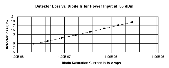
NOTE: There is an error in the title of the graph. It should read: Detector Loss vs. Diode Is for a DC Power Output of -66 dBm. I used the -66 dBm signal level for the graph because it is related to the weakest voice signal I can hear with my most sensitive headphones, and still understand about 50% of the words. Here is the listening experiment that I used to determine that power level. I fed my headphones directly from a transistor radio through my FILVORA and reduced the volume until I judged I could understand about 50% of the words of a voice radio program. This enabled me to determine the average impedance of the headphones. (See article #2). I then measured the p-p audio voltage (Vpp_audio) on the headphones with an oscilloscope. Assume the AM station was running at about 100% modulation. The peak instantaneous audio voltage at the detector will be equal to Vpp_audio since the modulation is 100%. Now make the assumption that a CW carrier is driving the detector at such a level that the DC output voltage (Vdc) at the detector is equal to Vpp_audio. That DC voltage across a resistor of value equal to the detector load resistance will deliver an output power of Pdc=10*log((1000*(Vdc^2))/Rload) dBm. Since I could not get into the radio to measure the actual detector voltages and the audio load resistance, I used the p-p voltage measured across my 1200 Ohm headphones in place of Vdc to calculate the instantaneous power at the modulation peaks. Pp=10*log(1000*((Vpp_audio^2)/1200= -66 dBm. This power, Pp is that used in calculating the graph above. In my case Vpp_audio = 0.00055 Volts and effective headphone impedance = 1200 Ohms. To calculate the actual audio power level I was using in the listening
experiment, I assumed that the demodulated audio voltage was a sine wave
(not
a voice) with the same p-p value as the actual measured voice p-p voltage.
It was then a simple matter to use the p-p voltage of the assumed audio
sine wave (Vpp_audio) and the effective impedance (PHI) of the headphones
to calculate the power of the audio sine wave in dBm. P=10*log ((1000*(Vpp_audio^2))/(8*PHI))
dBm. This value comes out 9 dB less than the DC power of -66 dBm.
Of course there is an error here in assuming that a sine wave of a specific
p-p voltage has the same RMS value as that of a broadcast voice waveform
of an equal p-p value. The "Audio Cyclopedia", in an article on VU
meters, states that the actual power from a voice signal is 8-10 dB less
than the power from a sine wave of the same p-p voltage. I'll use
9 dB. Bottom line: The audio power from a voice voltage waveform
is 18 dB less than the audio power from a sine wave voltage of p-p value
equal to the p-p voltage of the voice waveform. We can now calculate
that the electrical power of weakest voice audio signal I can barely understand
is -66 -9 -9 = -84 dBm. This figure depends on the sensitivity
of the headphones used and one's hearing acuity. I used a good
sound powered headphone set in this test. My hearing acuity is pretty
poor.
3. PRACTICE Keep in mind that diodes have an unavoidable back leakage resistance. Schottky diodes generally are very good in this respect. An exception is the so-called "zero bias" detector diodes. They have very high Is values and low reverse breakdown voltages and are generally not suitable for crystal radio. Germanium and cats whisker diodes are worse than Schottkys and vary greatly. This reverse resistance increases detector loss and reduces selectivity. "n" in the diode equation is usually close to 1.05 for Schottky barrier diodes. It is about 1.15 in Germanium diodes. All diodes have a fixed parasitic series resistance Rs. It is usually low enough to be ignored in crystal radios. One problem with Schottky diodes having a low reverse breakdown voltage and low Is is that they are more vulnerable to damage from static electricity than diodes with a higher leakage resistance. Tuned circuit loss and bandwidth considerations: A practical problem in using a diode of low Is is getting a high enough tuned circuit impedance for driving the diode. Of course, the first thing to do is to tap the diode all the way up on the output tuned circuit. An isolated tuned circuit having a typical Q of 350 at a frequency of 1.0 MHz, with a circuit capacitance of say 100 pF, and not coupled to an antenna or detector diode will have a resonant resistance of about 560k ohms. RF bandwidth will be fo/Q = 2.86 kHz. If an antenna resistance is now coupled in sufficiently to drop the resonant resistance by half to 280k, all of the available received RF power will be dissipated in the resonator, resulting in a bandwidth of 5.72 kHz (loaded Q of 175). If a diode is selected to match the now 280k ohm source resistance, it will present a 280k RF load resistance and result with a tuned circuit loaded Q of 87.5 giving an RF bandwidth of 11.4 kHz. The overall power loss caused by the tuned circuit loss is 3 dB. The diode will only receive 1/2 the maximum available-power at the antenna. The diode should have an Is of about n*0.026/278k = 100 nA (assuming a Schottky barrier diode is used). Note this: Even though the the diode is driven from a perfectly matched source (parallel connected combo of 560k tuned circuit loss and 560k antenna resistances), now the antenna does not see a matched load. It sees a parallel combo of the tuned circuit loss resistance of 560k and the 280k RF resistance of the diode. This is a resistance of 187k ohms. This mismatch power loss, included in the 3 dB above can be partially recovered by properly and equally mismatching the antenna and the diode. If this is done by more loss-less impedance transformation (technically, with an S parameter return loss of -11.7 dB), the total tuned-circuit power loss reduces to 2.63 dB, a reduction of 0.37 dB (pretty small, but it's there). If the ratio of unloaded to loaded tuned circuit Q was less than the 4:1 ratio used here, the loss reduction would be larger. Audio impedance transformation: One way to transform the 12k ohm effective impedance of a 2k ohm DC resistance Brandes Superior headset up to 280k ohms is to use an Antique Electronic Supply # P-T156, Stancor A53-C or similar 3:1 turns-ratio inter stage transformer. I measure an insertion power loss of only 0.5 dB with the following connection (See Articles #4 and #5 for other options.):
Note that the impedance transformation ratio is 16:1 thus stepping up the impedance of the 12,000 ohm headphones to 192,000 ohms not 278,000 ohms. This represents a mismatch of about 1.5:1. It will add a mismatch insertion power loss of only 0.15 dB. If the impedance mismatch had been 2:1, the insertion power loss would have been 0.5 dB. A 4:1 mismatch gives an insertion loss of 1.9 dB. The lead grounding the transformer lamination stack and frame is used if the transformer is mounted on an insulated material. It prevents the buildup of static charge on the frame during dry weather. Discharge of it might cause a crackling sound in the headphones or damage the diode (I got the crackling sound until I made the grounding connection). The transformer windings start and stop leads should be connected as shown to minimize the effect of the primary to secondary winding capacitance. If the f and s connections are reversed, the capacitance between the end of the secondary and the start of the primary winding will be across the primary and reduce the high frequency cut-off point. The lower impedance (secondary) winding is usually wound on the bobbin first, then after winding on several layers of insulation film, the higher impedance (primary) is wound. To determine how to connect the leads of the transformer, connect the primary and secondary windings as shown. (Disregarding the s and f notations). Connect an audio generator set to 1.0 kHz through a 200k ohm resistor. Load the secondary with a 12,000 Ohm resistor. Probe the input and output voltages with a scope. The output voltage should be about 0.25 of the input voltage. If the output voltage is about 0.5 that of the input, reverse the secondary leads. Repeat the test at 20,000 Hz and note the input and output voltages. Now reverse both the primary and secondary leads and repeat the 20 kHz test. The connection that gives the largest output voltage at 20 kHz is the correct one. Note that R3 is shown above as a rheostat not a fixed resistor. The nominal setting under the low signal level conditions discussed here is about 192k Ohms. Setting it to zero has little effect on reception of these low level signals. With this design approach, when receiving high level signals, RF selectivity is not reduced as much as when the DC resistance in the diode circuit is substantially below the effective impedance of the headset. When receiving very strong signals, R3 should be set for minimum distortion. One last comment: These design values are not critical. If impedances vary by several times from the optimum values, usually only a small sensitivity reduction will occur. What is the effect on the volume in the headphones of a change of X dB?
Many years ago I did a study which determined, in a blinded condition,
that a +1.0 dB or a -1.0 dB change in sound level was barely discernible
by most people. Half couldn't tell if the sound level was changed
or not after being told that a change might have occurred. Another
study had the listener listen to a sound. The sound was then turned
off for several seconds and then on again at the same level, at a level
of +3.0 dB or at a level of -3.0 dB. After the delay, only half
the listeners could tell whether the level of the sound had changed
or not. Incidentally, the listeners were not golden eared hi-fi
listeners. 4. SUMMARY
#1 Published: 07/15/99; Last revision: 02/12/2006 |