|
Design, construction and measurement of a single-tuned crystal radio set using a two-value inductor, along with a discussion of the cause of 'hash', short-wave ghost-signal and spurious FM reception. A way is presented for determining if the signal is operating a detector above or below its linear-to-square-law crossover pointBy Ben H. Tongue Means are provided for increasing selectivity at a small sacrifice in sensitivity. This crystal radio set is not designed to have strong immunity to local pick-up from local "blowtorch" stations. Selectivity and insertion power loss figures from a computer simulation are given and compared with those of the actual physical crystal radio set. A way to tell if the detector is operating below, at or above its 'Linear-to-Square Law Crossover point' (LSLCP) is described. No external antenna tuner is necessary. An explanation of 'short wave ghost signals' and 'hash' is provided along with some suggestions on how to combat them. This version 'b' uses only one diode and audio transformer configuration, as compared to the two used in the original obsolete version (now called Version 'a'). Also a new way to make a higher Q, low inductance coil using all the wire and coil form of the high inductance coil is described. Finally, the small performance sacrifice at the high end of the band that occurs when more readily available and lower cost parts are used is discussed. Additional benefits of the "Benodyne" type of tank circuit
are: (1) Reduction of the the sharp drop in tank Q or sensitivity at the high frequency
end of the BC band often experienced when only one value of tank inductance
is used for the whole BC band. (2) Reduction of the tank Q from loss
in the variable cap when using lower cost units that use phenolic
insulation, such as the common 365 pF cap (see Figs. 2, 3, 4, and 5 in Article #24). The "two inductance value benodyne* circuit is used in the crystal radio sets in Articles #22 and #26. We assume
here that the two "Benodyne" component inductors (see "The Tank Inductor"
in Article #26) provide a tank inductance of 250 uH in the low frequency
half of the BC band (520-943 kHz) and 62.5 uH in the high half (0.943-1.71
MHz). If the large 250 uH inductance setting were used all the
way up to the top end of the BC band (as in the usual case), a total
tuning capacity of 34.7 pF would be required at 1.71 MHz (Condition
A). In the "Benodyne" circuit, with the 62.5 uH inductance setting
used for the high frequency half of the BC band, a total tuning capacitance
of 139 pF is required at 1.71 MHz (Condition B). Benefit (1) occurs
because in condition A, a larger fraction of the total tuning capacitance
comes from the typically low Q distributed capacity of the inductor
than in condition B. This results in a higher Q total capacitance
in condition B than in condition A. Benefit (2) occurs because
The effective Q of a typical 365 pF variable cap, when used with a 250
uH tank, is about 500 at 1.71 MHz (see Fig. 3 in Article #24).
The Q of the 365 pF variable cap, when set to 139 pF, is greater than
1500 (see Fig.5 in Article #24). This higher Q results in less
loss and greater selectivity at the high end of the BC band in condition
2. A further benefit of the Benodyne circuit at the high end of
the BC band is greater immunity from the Q reducing effects of surrounding
high loss dielectric materials such as baseboard etc. The lossy
stray capacity introduced is better swamped out by the high shunt tuning
capacity used. The Crystal Radio Set Design, in a (large) Nutshell:
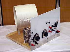
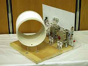
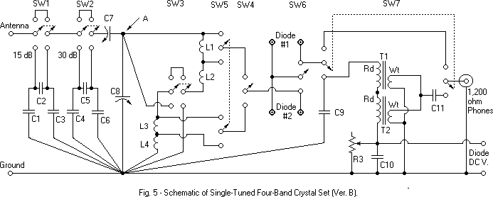
Fig. 1 - Single-Tuned Four-Band Crystal Radio Set, Version 'B'. The design objectives for the crystal radio set are:
1. Theory
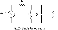
The frequency response shape of the circuit shown in Fig. 2 is that of a simple single tuned circuit and can be thought of as representative of the nominal response of a single tuned crystal radio set. Consider these facts:
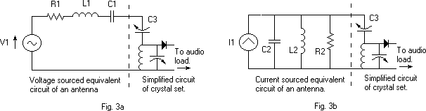
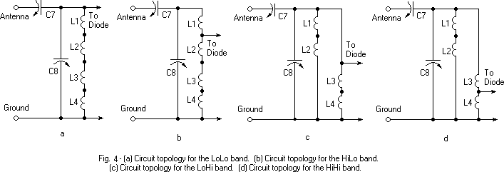
Fig. 3a shows the simplified Standard Dummy Antenna circuit, described in Terman's Radio Engineer's Handbook, for simulating a typical open-wire outdoor antenna-ground system in the AM band. R1=25 ohms, C1=200 pF and L1=20 uH. See Article #20 for info on how to measure the resistance and capacitance of an antenna-ground system. The values shown for Fig. 3a are used in the design of the crystal radio set. R1 represents primarily the ground system resistance. C1 represents the capacitance of the horizontal wire and lead-in to ground and L1 represents the series inductance of the antenna-ground system. The values of R1, C1 and L1 in Fig. 3a will be considered to be independent of frequency. To the extent that they do vary with frequency, C7 and C8 in Fig. 5 can be adjusted to compensate. The current-source equivalent circuit of the antenna-ground circuit is shown in Fig. 3b. To a first degree of approximation, in the practical case, C2 in Fig. 3b is independent of frequency. R2 will vary approximately inversely with frequency. We will ignore the effect of L2, since its value is large, except when approaching the first resonance of the antenna-ground system. The design approach is to place a variable capacitor C3 in series with the antenna circuit (Fig. 3a) to enable impedance transformation of the antenna-ground circuit to an equivalent parallel RC (Fig. 3b), the R component of which can be adjusted by changing the value of the C3 to follow a desired relationship vs frequency. One of the objectives of the design is to enable as constant a bandwidth as possible vs. frequency. This requires the aforementioned equivalent parallel R2 component to vary proportionally with the square of the frequency if capacitive tuning is used as it is here, in each sub-band (Q must be proportional to frequency for a constant bandwidth). This design attempts to accomplish this in the center of each frequency band. Performance is close at band edges. 3. The single tuned crystal radio set The topology of the single tuned circuit is changed from band to band as shown in Fig. 4 below.
The resonant RF resistance values at the top of C8 (Fig. 4), from the transformed antenna resistance, (at the center of each sub-band) are designed to be: 250k ohms for bands LoLo and LoHi, and 500k ohms for bands HiLo and HiHi. Since the diode is tapped at the 0.7 voltage point for bands HiLo and HiHi, it sees a source resistance at resonance of: 125k for bands LoLo and LoHi and of 250k ohms for bands HiLo and HiHi. These figures apply for the theoretical case of zero loss in the tuned circuits (infinite Q). In a shunt capacitively tuned crystal radio set, loaded with a constant resistive load, the bandwidth will vary as the square of the frequency. To understand why, consider this: When the resonant frequency of a tuned circuit loaded by fixed parallel resistance is increased (from reducing the total circuit tuning capacitance), the shunt reactance rises proportionally, giving rise to a proportionally lower circuit Q. But, a proportionally higher Q is needed if the bandwidth is to be kept constant. There for, the square relation. In the practical case, we are faced with two problems. (1) How should we deal with the fact we work with finite Q components? (2) At high signal levels (above the LSLCP), the RF load presented by the diode to the tuned circuit is about 1/2 the audio load resistance, and at low signal levels (below the LSLCP) the RF load presented to the diode is about 0.026*n/Is ohms. Compromises are called for.
Parts List - All components are chosen for the best possible sensitivity at a -3 dB RF bandwidth of 6 kHz (except for not using litz wire in the inductor).
** For lower cost, the following component substitutions may be made: Together they cause a small reduction in performance at the high end of the band (about 1.75 dB greater insertion power loss and 1.5 kHz greater -3 dB bandwidth). The performance reduction is less at lower frequencies.
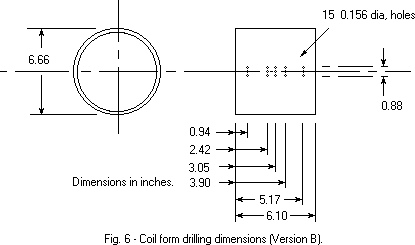
The coil should be mounted with its axis at a 30 degree
angle to the front panel as shown in Fig.1. The center of the coil
form is 2 7/8" back from the rear edge of the baseboard and 5 5/8" to
the left of its right edge. These dimensions are important,
as is the actual size of the breadboard, if one wishes to construct a
double-tuned four band crystal radio set out of two Version 'b' single-tuned
four band crystal radio sets as described in Article #23.
The diode: This design is optimized for use with a diode having an n of 1.03 and a Saturation Current (Is) of about 82 nA, although this is not critical and other diodes can be used with good results. See Articles #0, #4 and #16 for info on n and saturation current (Is) of diodes, and how to measure them. If desired, and one has a favorite diode, its effective (Is) can be changed by applying a DC bias voltage, using perhaps, the 'Diode Bias Box' described in Article #9. One suitable diode, the published parameters of which show an (Is) of 100 nA is a Schottky diode, the Agilent HBAT-5400. It is a surface-mount unit that was originally designed for transient suppression purposes. Measurements of many HBAT-5400 diodes seems to show that there are two varieties. One type measures approximately: n=1.03 and (Is)=80 nA. The other type seems to have an n of about 1.16 and an (Is) of about 150 nA. Both work well but the former works the best. This part, available in an SOT-23 package is easily connected into a circuit when soldered onto a "Surfboard" such as manufactured by Capital Advanced Technologies (http://www.capitaladvanced.com/), distributed by Alltronics, Digi-Key and others. Surfboard #6103 is suitable. The HBAT-5400 is also available in the tiny SO-323 package that can be soldered to a 330003 Surfboard. The Agilent HSMS-2860 microwave diode (Specified Is=50 nA) is available as a single or triple with three independent diodes in the SO-323 and SO-363 packages, respectively. The Agilent number for the triple diode is HSMS-286L. I find it to be particularly good for DX in this crystal radio set. It is a convenient part since one can connect it using only one section (shorting the unused ones) or with two or three in parallel. This gives one a choice of nominal saturation currents of 50, 100 or 150 nA. Samples of this part I have tested measured about 35 nA per diode, not 50. I don't know the normal production variations. The only disadvantage of this diode, as far as I know, is its low reverse breakdown voltage which may cause distortion and low volume on very loud stations. It has the advantage, as do most Schottkys, of having much less excess reverse leakage current than do germanium diodes. This helps with volume and selectivity on very weak stations. Infineon makes a BAT62 Schottky diode in several different quite small surface mount packages. The single BAT62 is physically the largest. It has a specified (Is) of about 100 nA and performs quite well. Be forewarned that the diode parasitic series resistance is a high 100 ohms in this diode. A resistance even this high should not have a noticeable effect on the performance of a crystal radio set. Most germanium diodes have too high a saturation current for the best selectivity and should to be back-biased or cooled for optimum performance. See Article #17A for more info on this. Different type diodes may be connected to the terminals labeled Diode #1 and Diode #2, with either one selectable with SW6. When one diode is selected, the other is shorted. This feature makes it easy to compare the performance of a 'test' diode with one's 'favorite' diode. Another use is to place one's best DX diode in one position and one having a very low reverse leakage resistance at high reverse voltages in the other. This will maximize strong signal volume and minimize audio distortion. A good choice for this crystal radio set is a diode having a relatively low saturation current such as 3 or 4 Agilent HSMS-2820 or HSMS-2860 diodes in parallel as Diode #1 for high selectivity and sensitivity on weak signals, and an Agilent HBAT-5400 or one of the lower saturation current germaniums as Diode #2 for low distortion and maximum volume on strong stations. Don't use two diodes in series if you want the best weak signal sensitivity in any crystal radio set. The result of using two identical diodes in series is the simulation of an equivalent single diode having the same (Is) but an n of twice that of either one. This reduces weak signal sensitivity. The inductor for this single tuned crystal radio set is made up of the four closely coupled inductors L1, L2, L3 and L4. The inductance from point A to ground (Fig. 5) is 250 uH when SW3 is in the 'up' position (used for low band reception) and 62.5 uH in the 'down' position (used for high band reception). Better performance from a higher tank Q at the high frequency end of band B may be obtained by using the "contra-wound" coil winding technique described in Article #26. This minimizes distributed coil capacitance in band B as opposed to the winding connections used here that minimize coil distributed capacity in band A. Audio impedance transformation from the audio output resistance of the diode detector to 'series connected' 1.2k ohm sound-powered phones is provided by the audio transformers. If one wishes to use 300 ohm sound-powered phones with two 600 ohm elements connected in parallel instead of series, a very good low loss transformer choice is the 100k-100 ohm transformer from Fair Radio Sales, #T3/AM20. The configuration of two Calrad transformers shown on line 2 of the Calrad chart in Article #5 is also a good choice. C11, along with the shunt inductance of the transformer and the inductance of the sound powered phones form a high-pass filter, hopefully flat down to to 300 Hz. R3 is used to adjust the DC resistance of the diode load to the AC impedance of the transformed effective AC headphone impedance. C10 is an audio bypass. The two variable capacitors C7 and C8 interact substantially when tuning a station. C7 mainly controls the selectivity and C8 mainly controls the resonant frequency. If the antenna-ground system being used has a resistance larger than 25 ohms, C7 will have to be set to a smaller capacitance in order to maintain the proper resonant resistance at point A in Fig. 5. If the capacitance of the antenna-ground system is greater than 200 pF, C7 will also have to be set to a lower value than if it were 200 pF. The "capacitive" attenuators controlled by SW1 and SW2, used for volume and selectivity control, are designed so as to cause minimal tank circuit detuning when the equivalent circuit of the antenna-ground system used has the same values as the old IRE simplified Dummy Antenna recommended for testing Broadcast Band radio receivers. It consisted of a series combination of a 200 pF cap, 20 uH inductor and a 25 ohm resistance. The geometric mean of the sum of the reactances of the capacitor and inductor at 520 and 1710 kHz is (-605) ohms. This is the reactance of a 279 pF capacitor (characteristic capacitance of the "capacitive" attenuator) at 943 kHz, the geometric mean of the BC band of 520-1710 kHz. The "capacitive" attenuators were designed for the specified attenuation values (15 and 30 dB) utilizing the 500 ohm resistive pi attenuator component values table shown in the book "Reference Data for Radio Engineers". The resistor values for 15 and 30 dB "capacitive" attenuators were normalized to 605 ohms, then the "capacitive" attenuator capacitor values were calculated to have a reactance, at 943 kHz, equal to the value of the corresponding "capacitive" attenuator shunt or series resistance. Since the "capacitive" attenuators, when switched into the circuit, isolate the antenna-ground system resistance from the tank circuit, selectivity is increased. This is a convenient feature, since less retuning is required than if selectivity is increased by reducing C7 and increasing C8. If the series capacitance of the equivalent circuit of one's own antenna-ground system is 200 pF, at 943 kHz, practically no retuning is required. If the equivalent L and C of one's own antenna-ground system differ substantially from those of the simplified IRE dummy antenna used here, one can normalize the values of the capacitors used in the "capacitive" attenuators to match ones's own antenna-ground system. A method for measuring the parameters of one's own antenna-ground system is shown in Article #20. 4. 'Loop Effect' of the tank inductor,
and how it can be used to tame One can use local signal pickup by the tank (loop effect) to reduce the effect of interference from strong stations by rotating the crystal radio set about a vertical axis. The correct angle will generally reduce it. 5. How to improve selectivity with a relatively small loss in sensitivity.
Note: When altering selectivity by changing switch positions, always
re-balance the relative settings of C7 and C8. 6. Just how loud is a station that delivers the amount of power necessary to operate the Diode Detector at its 'Crossover Point' between Linear and Square-Law Operation? Many Articles in this series have talked about the 'Linear-to-Square-Law Crossover Point' (LSLCP). Please bear in mind that the LSLCP point is a point on a graph of output DC power vs input RF power of a diode detector system. It is not a point on a graph of DC current vs voltage of a diode. Two things can be said about a detector when it is fed a signal that operates it at its LSLCP. (1) A moderate increase of signal power will move the detector into its region of substantially linear operation. (2) A similar moderate decrease of input power will move it closer to its region of substantially square law operation, where a 1 dB decrease of input power results with a 2 dB decrease of output power. For more info on the LSLCP, see Article #15A. The crystal radio set described in this Article is operating at its LSLCP if the rectified DC voltage at the 'Diode Bias' terminals is 53 mV, a diode having a Saturation Current (Is) of 82 nA and an ideality factor (n) of 1.03 is used (such as a selected Agilent HBAT-5400), and if R3 is set to 325k ohms. At this point the diode rectified current equals two times its Saturation Current. The volume obtained is usually a low to medium, easy-to-listen-to level. 7. 'Short Wave ghost Signal', 'background hash' and spurious FM reception. All single tuned crystal radio sets may be, in fact, considered double tuned (except single tuned loop receivers). The second response peak arises from resonance between the equivalent inductance of the antenna-ground system and the impedance it sees, in this case, the series combination of capacitors C7 and C8. This peak usually appears at a frequency above the broadcast band and gives rise to the possibility of strong so-called 'short wave ghost' signal interference when a short wave station has a frequency near the peak . The response at this ghost frequency can be made somewhat weaker and moved to a higher frequency if the antenna-ground system inductance is reduced. One can use multiple spaced conductors for the ground lead to reduce its inductance. I use a length of TV 300 ohm twin lead, the two wires connected in parallel for this purpose. Large gauge antenna wire, or spaced, paralleled multiple strands helps to reduce the antenna inductance (flat top antenna). If the down-lead is long compared to the ground lead, use multiple, paralleled, spaced conductors to reduce its inductance (similar to using a 'cage' conductor). Another possible cause of 'ghost' signal reception resides in the fact that the response of the so-called single tuned circuit does not continuously drop above resonance as frequency rises, but only drops to a relatively flat valley before rising again to the second peak. The frequency response above the main (lower) peak would drop monotonically (true single tuned operation) if the second peak did not exist. The relatively flat response valley that exists between the two peaks, provides the possibility (probably likelihood) of interference 'hash' if several strong stations are on the air at frequencies in the valley range. It also is the cause of a strong local station, above the frequency of a desired station "riding through" and appearing relatively constant even if the tuning dial is moved. The response should drop at a 12 dB per octave rate above the second peak. A useful side effect of the response behavior of this type of circuit is that the response below the main resonance drops off at an extra fast rate of 12 dB per octave rate instead of an expected 6 dB. The most effective way to substantially eliminate 'short wave ghost' and hash reception is to go to a double-tuned circuit configuration or to use traps. Spurious FM reception caused by so-called FM 'slope' detection can occur from close by local FM stations if a spurious FM resonance appears somewhere in the circuitry of a crystal radio set. If ground wiring is not done properly in the crystal radio set, spurious signals can get into the detector. The thing to do here is to run all the RF and audio grounds to one point as shown in Fig.5. Sometimes a small disc bypass capacitor, 22 pF or so, placed across the diode will help. Another way to try to reduce FM interference is to put a wound ferrite bead 'choke' in series with the antenna and/or ground leads. In order not to affect normal BC band reception, the resultant ferrite inductor should have a reasonable Q and a low inductance in the BC band. It should also exhibit a high series resistance at FM frequencies. Suitable wound ferrite chokes (bead on a lead) are made by the Fair-Rite Corp. as well as others. Two types available from Mouser are #623-29441666671 and #623-2961666671. This suggestion may also help reduce "short wave ghost" signal reception. 8. Some simulated and actual measurements on the crystal radio set.
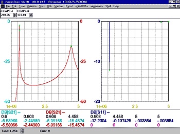
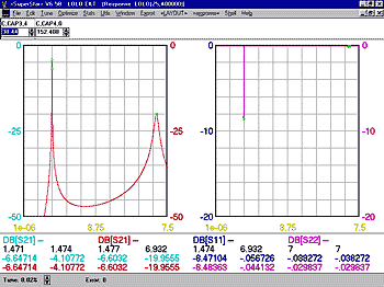
Fig. 7 shows the simulated frequency response at the center of the LoLo band, from the antenna source to the RF input of the diode. The red graph and figures in the left panel show an insertion power loss of 2.4 dB with a -3 dB bandwidth of 6 kHz, along with the spurious response peak at 4.4 MHz, caused by the antenna-ground system inductance. The insertion loss at the spurious peak is 15 dB. The loss in the valley is 40 dB. The right graph and figures show the Input Return Loss (impedance match) at resonance to be -12.2 dB. The output return loss (not shown) is the same. Fig. 8 shows the simulated frequency response at the center of the HiHi
band, from the antenna source to the RF input of the diode. The
red graph and figures in the left panel show an insertion power loss of
4.1 dB with a -3 dB bandwidth of 6 kHz, along with the spurious response
peak at 6.9 MHz, caused by the antenna-ground system inductance.
The insertion loss at the spurious peak is 20 dB. The loss in the
valley is 47 dB. The right graph and figures show the Input Return Loss
(impedance match) at resonance to be -8.5 dB. The output return
loss is the same.
9. A method for measuring the unloaded Q of an L/C resonator.
10. Important information re: unloaded tank Q. Every effort should be made to achieve as high an unloaded tank Q as possible, in order to minimize RF loss at the desired -3 dB bandwidth (selectivity), and especially when using narrower bandwidths. Somewhat greater insertion power loss and/or broader selectivity may result if components having a greater dielectric loss than those specified are used. Sensitive areas for loss are:
11. Measurements.
In use, C7 and C8 are usually set to different values to achieve the design-bandwidth of 6-7 kHz. However, if they are set to the same values, a frequency calibration chart can be made for each band as shown above. The bold figures indicate the approximate position of each band when the crystal radio set is driven by the standard antenna-ground system. There is sufficient extra capacitance range available in C7 and C8 to handle antenna-ground systems that differ substantially in impedance from the standard dummy antenna used in the design.
The data in Table 4 shows the insertion power loss in the crystal radio set when driven by an RF signal that is amplitude modulated at 50% by a 400 Hz sine wave. See Article #11 on how to measure the insertion power loss and bandwidth of a crystal radio set. The audio output power was set to -70 dBW for each reading. The available carrier input power supplied to the crystal radio set was about -60 dBW, with a total available sideband power of about -66 dBW. The audio output power is that delivered by the diode detector to the audio load and does not include losses in an audio transformer. One should add about 1.0-1.5 dB to the insertion power loss shown in Table #4 to allow for audio transformer loss. The reason the audio transformer loss does not show up in the measurements is that the audio transformers (T1 and T2) were not used. SW7 was placed in the UP position, providing a direct high impedance output from the diode detector. The Zero Loss Unilateral 'Ideal Transformer' Simulator described in Article #14 was used to provide a 320k to 1200 ohm impedance transformation, close to that provided by T1 and T2 in actual crystal radio set operation. Note: The diode rectified DC voltage at the power levels used above is 0.51 volts. At this power level, a SPICE simulation of the detector shows a theoretical diode detector insertion power loss of 1.4 dB. #22 Published: 02/05/2002; Revised:08/20/2006 | |||||||||||||||||||||||||||||||||||||||||||||||||||||||||||||||||||||||||||||||||||||||||||||||||||||||||||||||||||||||||||