Highly sensitive and selective single-tuned four-band crystal radio set using a new contra wound dual-value inductor, and having a 'sharp selectivity setting'; along with a way to measure the unloaded Q of an L/C resonator
By Ben H. Tongue
Summary: This article describes Version 'c' of
a single-tuned four-band crystal radio set, sometimes called a "Benodyne"
(constant bandwidth with maximum weak-signal sensitivity across the whole BC band, achieved by using 2 or more values of inductance in the tank - lower values at higher frequencies). It is designed for a constant bandwidth
across the AM band, two selectivity settings (normal and sharp) and low
loss (high sensitivity) especially for weak signals at the high end of the band. It is an attempt to achieve the two objectives
at a -3 dB RF bandwidth of about 5-6 kHz (relatively independent of signal
strength), with a constant high efficiency across the entire AM broadcast
band (normal selectivity setting): 1) Best possible sensitivity
on weak signals, 2) Loudest possible volume on strong signals. The
sharp selectivity setting reduces the -3dB bandwidth to about 2 kHz, but
unavoidably introduces some extra insertion power loss.
Selectivity and insertion power loss figures from a computer simulation are given and compared with those of the actual physical crystal radio set. A way to tell if the detector is operating below, at or above its 'Linear-to-Square Law Crossover point' (LSLCP) is described. See Article #15a for a discussion of LSLCP. No antenna tuner is necessary for the average outdoor or attic antenna. An explanation of 'short wave ghost signals' and 'hash' is provided along with some suggestions on how to combat them. Version C uses a tank coil constructed with litz wire, as compared to the solid teflon insulated wire used on version 'B'. A new way to make a higher Q, low inductance coil is described.
Some additional benefits of the "Benodyne" type of tank
circuit are: (1) Reduction of the the sharp drop in tank Q or sensitivity at the high
frequency end of the BC band often experienced when only one value of
tank inductance is used for the whole BC band. (2) Reduction of the tank
Q loss from the variable cap when using lower cost units that use phenolic
insulation, such as the common 365 pF cap (see Figs. 2, 3, and 4 in Article #24). The "two inductance value benodyne* circuit
is used in the crystal radio sets in Articles #22 and #26. We will assume
here that the two "benodyne" component inductors (see "The Tank Inductor"
in this Article) provide a tank inductance of 250 uH in the low frequency
half of the BC band (520-943 kHz) and 62.5 uH in the high half (0.943-1.71
MHz). If the large 250 uH inductance setting were used all the way
up to the top end of the BC band (as in the usual case), a total tuning
capacity of 34.7 pF would be required at 1.71 MHz (Condition A). In the
"Benodyne" circuit, with the 62.5 uH inductance setting used for the high
frequency half of the BC band, a total tuning capacitance of 139 pF is
required at 1.71 MHz (Condition B). Benefit (1) occurs because in
condition A, a larger fraction of the total tuning capacitance comes from
the typically low Q distributed capacity of the inductor than in condition
B. This results in a higher Q total capacitance in condition B than
in condition A. Benefit (2) occurs because the effective Q of a
typical 365 pF variable cap, when used with a 250 uH tank, is about 500
at 1.71 MHz (see Fig. 3 in Article #24). The Q of the 365 pF variable
cap, when set to 139 pF, is greater than 1500 (see Fig.5 in Article #24).
This higher Q results in less loss and greater selectivity at the high
end of the BC band in condition 2. A further benefit of the Benodyne
circuit at the high end of the BC band is greater immunity from the Q
reducing effects of surrounding high loss dielectric materials such as
baseboard etc. The lossy stray capacity introduced is better swamped
out by the high shunt tuning capacity used.
The Crystal Radio Set Design, in a (large) Nutshell:
- The design approach is to divide the AM band into several sub-bands in an attempt to keep the selectivity relatively constant and the insertion power loss low across the whole band.
- The first step is to divide the BC band into two halves: band A (520-943 kHz) and band B (943-1710 kHz). Two-step shunt inductive tuning is employed to switch between bands. A tank inductance of 250 uH is used in band A and 62.5 in and B.
- Band A is further subdivided into two bands: sub-bands 1 (520-700 kHz) and 2 (700-943 kHz). The band B is also subdivided into two bands: sub-band 3 (943-1270 kHz) and 4 (1270-1710 kHz).
- In the normal selectivity mode, two different resonant RF resistance levels, measured at the top of the tuned circuit (point 'A' in Fig. 5), are used at the center of the sub-bands. This impedance level is about 125k ohms at the center of sub-bands 1 and 3. It is 250k at the center of sub-bands 2 and 4 (excluding the resistive losses of the components used). These resistance values are made up of a parallel combination of the transformed RF antenna-ground system resistance and the input RF resistance of the diode. These two resistances should be equal to each other to achieve minimum insertion power loss, at the design bandwidth. This means that the transformed antenna-ground system and diode RF resistances are each about 250k in sub-bands 1 and 3 and 500k in sub-bands 2 and 4 at point 'A'. The two different transformed RF antenna-ground system resistance values are achieved by proper adjustment of a variable capacitor in series with the antenna (C7 in Fig. 5). The higher diode RF tank loading resistance value for sub-bands 2 and 4 are achieved by tapping the diode onto the tank at a point that is 70% of the turns up from ground. The tank is not tapped for sub-bands 1 and 3 and connection is to the top of the tank. In the sharp selectivity mode the diode is tapped half of the turns down on the tank from the point used for normal selectivity.
- The weak-signal RF input and audio output resistances of a diode detector are approximately the same and equal to 0.026*n/Is ohms (Is means diode saturation current, see Article #0-Part 4). The strong-signal audio output resistance of a diode detector is approximately equal to 2 times the RF resistance of its source. Compromise audio impedance transformation ratios are used to optimize performance on both weak and strong signals.
- The design is scalable. Less expensive parts that may have somewhat greater losses may be used with some penalty in sensitivity and selectivity, especially at the at the high end of the BC band and at the Sharp Selectivity setting. See the Parts List for a listing of some more easily available and lower cost parts than the ones used in the original design.
 |
 |
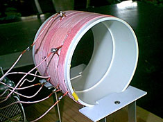 |
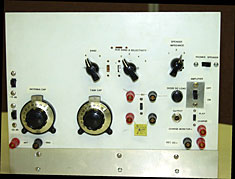
Fig. 1 - Single-Tuned Four-Band Crystal
Radio Set, Version 'C'. These are actually pictures of Version B as
described in Article #22, converted to version C, as described in this
Article, but modified with the
addition of the amplifier in Article #25. This Article does not
include the amplifier.
Design objectives:
- A relatively constant -3 dB bandwidth of 5 to 6 kHz across the full range of 520 to 1710 kHz at normal selectivity, with a relatively constant RF power loss in the RF tuned circuits of less than 3 dB.
- A switched adjustment to achieve about 3 times sharper selectivity than normal.
- Optimal performance with external antenna-ground systems having a fairly wide range of impedance.
- To provide a simple-to-use switching setup for comparing a 'test' diode with a 'standard' one.
- To provide a volume control with a range of 45 dB in 15 dB steps that has the minimal possible effect on tuning, This was incorporated in the design because the two local 50 kW blowtorch stations WABC and WOR (about 10 miles away) deliver a very uncomfortably loud output from SP headphones from my attic antenna. A means of volume reduction that did not reduce selectivity was needed. This method of volume reduction actually increases selectivity by isolating antenna-ground resistance from the tank circuit.
- Introduction fo a new (to me) method for constructing low inductance high Q coils.
1. Theory
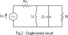
The frequency response shape of the circuit shown in Fig. 2 is that of a simple single tuned circuit and can be thought of as representative of the nominal response of a single tuned crystal radio set. Consider these facts:
- If Lt and Ct have no loss (infinite Q), zero insertion power loss occurs at resonance when Rs equals Rl. This is called an 'impedance matched' condition. The power source (Vs, Rs), looking towards the tank, sees a resistance value equal to itself (Rl). Also, the load (Rl), looking towards the input sees a resistance (Rs), equal to itself. In the practical case there is a finite loss in Lt and CT This loss can be represented by an additional resistance Rt (not shown), shunted across the tuned circuit. The input resistance seen by (Vs, Rs) is now the parallel combo of Rt and Rl and it is less than Rs The perfect impedance match seen by (Vs, Rs) when the tank Q (Qt) was infinite is now destroyed. The impedance matched condition can be restored by placing an impedance transformation device between the source, (Vs, Rs) and the tank.
- In Fig. 2, if tuning could be done with Lt alone, leaving CT fixed, the bandwidth would be constant. The problem here is that high Q variable inductors that can be varied over an approximately 11:1 range, as would be needed to tune from 520 to 1710 kHz do not exist. On the other hand, tuning by varying CT by 11:1 will cover the range, but have two disadvantages. (1) The -3dB bandwidth will vary by 1:11 from 520 to 1740 kHz. (2) In the practical case, if the bandwidth is set to 6 kHz at the low end of the BC band, and an attempt is made to narrow the bandwidth at 1710 kHz by placing a capacitor in series with the antenna, the insertion power loss will become great.
- The compromise used here is a coil design that can be switched between two inductance values differing by 4:1. The high inductance setting is used for the low half of the BC band and the low inductance for the high half. Capacitive tuning is used to tune across each half. The new technique used here, of using a combination of two inductors, enables the Q of the low value inductance (used in the high half of the band) to to be much higher than would be the case if a single coil of the same diameter and wire size, but with fewer turns, were used. This technique uses two coils, closely coupled, and on the same axis. They are connected in series to obtain the large inductance and in parallel for realization of the small one. The small inductance has a value 1/4 that of the large one and about the same Q at 1 MHz. (if coil distributed capacity is disregarded). The innovation, so far as I know, is to use the full length of wire used in the high inductance coil, occupy the same cubic volume, but get 1/4 the inductance and keep the same Q as the high inductance coil (at the same frequency). See Table 4.
- The high and low bands are each further subdivided giving a total of four sub-bands (1, 2, 3 and 4). If this were not done, we would be faced with a bandwidth variation of about 1:3.3 in each band. The geometrically subdivided bands are: sub-band 1 (520-700 kHz), 2 (700-943 kHz), 3 (943-1270 kHz) and 4 (1270-1710 kHz). The bandwidth should vary about 1:1.8 across each of these sub-bands. The bandwidths at the center of each of the four sub-bands are made approximately equal to each other by raising the loading resistance of the antenna-ground system and the diode on the tank by a factor of two in sub-bands 2 and 4, compared to the value used in sub-bands 1 and 3.
2. Design Approach for the Center of each of the four sub-bands.
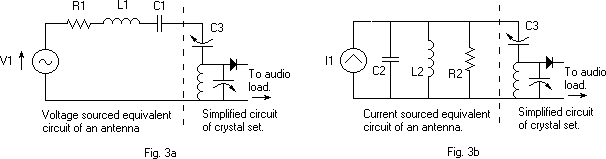
Fig. 3a shows the simplified Standard Dummy Antenna circuit, described in Terman's Radio Engineer's Handbook for simulating a typical open-wire outdoor antenna-ground system in the AM band. R1=25 ohms, C1=200 pF and L1=20 uH. See Article #20 for info on how to measure the resistance and capacitance of an antenna-ground system. These values are used in the design of the crystal radio set. R1 represents the antenna-ground system resistance, C1 the capacitance of the horizontal wire and lead-in to ground and L1 represents the series inductance of the antenna-ground system.
The values of R1, C1 and L1 in Fig. 3a are considered to be independent of frequency. To the extent that they may vary with frequency, C7 and C8 in Fig. 4 can be adjusted to compensate. The current-source equivalent circuit of the antenna-ground circuit is shown in Fig. 3b. To a first degree of approximation, C2 in Fig. 3b is independent of frequency. R2 will vary approximately inversely with frequency. We will ignore the effect of L2, since its value is large, except when approaching the first resonance of the antenna-ground system. The design approach is to place a variable capacitor C3 in series with the antenna circuit (Fig. 3a) to enable impedance transformation of the antenna-ground circuit to an equivalent parallel RC (Fig. 3b), the R component of which can be adjusted by changing the value of the C3 to follow a desired relationship vs frequency. One of the objectives of the design is to enable as constant a bandwidth as possible vs. frequency. This requires the aforementioned equivalent parallel component (R2) to vary proportionally with the square of the frequency if capacitive tuning is used in each sub-band (loaded Q must be proportional to frequency for a constant bandwidth). The shunt variable capacitor to ground, shown across the tank coil, is used to tune the tank to resonance. This design attempts to accomplish this in the center of each sub-band. Performance is close at the band edges.
3. The single tuned crystal radio set
The topology of the single tuned circuit is changed from band to band as shown in Fig. 4 below.
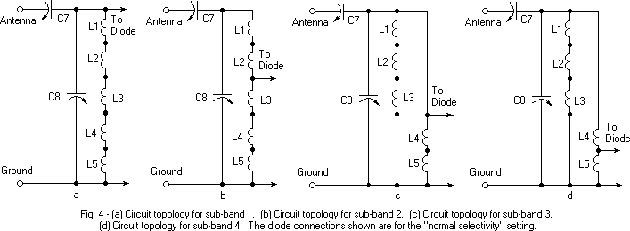
Resonant RF resistance values at the top of C8 (Fig. 4) from antenna loading are designed to be: 250k ohms at the center of sub-bands 1 and 3 and 500k ohms for sub-bands 2 and 4. Since the diode is tapped at the 0.7 voltage point for bands 2 and 4, it sees a source resistance at resonance of: 125k for sub-bands 1 and 3 and of 250k ohms for sub-bands 2 and 4. These figures apply for the theoretical case of zero loss in the tuned circuit components (infinite Q). In a shunt capacitively tuned crystal radio set, loaded with a constant resistive load, the bandwidth will vary as the square of the frequency. To understand why, consider this: When the resonant frequency of a tuned circuit loaded by fixed parallel resistance is increased (from reducing the total circuit tuning capacitance), the shunt reactance rises proportionally, giving rise to a proportionally lower circuit Q. But, a proportionally higher Q is needed if the bandwidth is to be kept constant. Therefore, the square relation.
In the practical case, we are faced with two problems. (1) How should we deal with the fact we work with finite Q components? (2) At high signal levels (above the LSLCP), the RF load presented by the diode to the tuned circuit is about 1/2 the audio load resistance, and at low signal levels (below the LSLCP) the RF load presented by the diode is about 0.026*n/Is ohms. Compromises are called for.
Parts List - All components are chosen for the best possible sensitivity at a -3 dB RF bandwidth of 5-6 kHz.
- C1, C3: 200 pF NPO ceramic caps.
- C2: 100 pF NPO ceramic cap.
- C4, C6: 270 pF ceramic caps.
- C5: 18 pF NPO ceramic cap.
- ** C7 (Antenna cap.), C8 (Tank cap.): 12-475 pF single section variable capacitors, such as those that were mfg. by Radio Condenser Corp. (later acquired by TRW). They use ceramic stator insulators and the plates are silver plated. Purchased from Fair Radio Sales Co. as part #C123/URM25. Other capacitors may be used, but those with phenolic stator insulators will cause some reduction of tank Q, especially at the high end of sub-band 4. The variable capacitors are fitted with 8:1 ratio vernier dials calibrated 0-100. These are available from Ocean State Electronics as well as others. An insulating shaft coupler is used on C7 to eliminate hand-capacity effects. It is essential, for maximum sensitivity and selectivity, to mount C7 in such a way that stray capacity from its stator to ground is minimized. See Part 11 for info on mounting C7. The variable capacitors used in this design may not be available now. Most any other capacitor with ceramic insulation should do well. Note: If one has available two capacitors having different losses for use as C7 and C8, the best one should be used for C8 since the sensitivity of this crystal radio set is less affected by a Q reduction of C7 than of C8.
- C9: 47 pF ceramic cap.
- C10: 0.1 to 0.22 uF cap.
- C11: Approx. 1.0 uF non-polarized cap. This is a good value when using RCA, Western Electric or U. S. Instruments sound powered phones with their 600 ohm elements connected in series. The best value should be determined by experiment. If 300 ohm sound powered phones having their 600 ohm elements connected in parallel are used, C11 should be about 4 uF and a different transformer configuration should be used.
- **L1, L2, L3, L4, and L5: See "The tank inductor" below.
- **SW1, SW2 and SW6: DPDT general purpose slide switches. Radio Shack mini DPDT switches from the #275-327B assortment or Switchcraft #46206LR are relatively low loss units.
- **SW3 (Used to switch between bands A and B): 5 position two pole ceramic insulated with silver plated contacts rotary switch, used as a 2 position 2 pole switch. For low loss, it is essential that the switch use ceramic insulation.
- **SW4 (Used to select a sub-band and switch between normal and sharp selectivity): 5 position single pole ceramic insulated rotary switch. For low loss, it is essential that the switch use ceramic insulation.
- **SW5: Switchcraft #56206L1 DPDT mini Slide switch. Used as a SPDT switch. This switch has unusually low contact resistance and dielectric loss, but is expensive. Other slide switches can be used, but may cause some reduction of tank Q.
- T1, T2: Calrad #45-700 audio transformers. Available from Ocean State Electronics, as well as others. If 300 ohm phones are to be used, see "Audio impedance transformation", below.
- R3 (used to adjust the resistive load on the diode): 1 Meg Pot., preferably having a log taper.
- Baseboard: 12'' wide x 11 1/8 '' deep x 3/4" thick.
- Front panel is made of 0.1" thick high-impact styrene. Other materials may be used. This is the the lowest loss practical material I could obtain.
** For lower cost, the following component substitutions may be made: They cause a reduction in performance at the high end of the BC band, especially, sub-band 4 when the "narrow selectivity" setting is used. Performance reduction is much less in the lower sub-bands and in the "normal selectivity setting.
- Mini air-variable 365 pF caps sold by many distributors such as The Crystal Set Society and Antique Electronic Supply may be used in place of the ceramic insulated ones specified for C7 and C8. Their maximum capacitance of 365 pF may not be large enough to enable achieving the design bandwidths at the lower end of bands A and B, especially when short antennas are used. This problem can be solved by making provision for switching a 220 pF NPO (sometimes called COG) disc capacitor across C7 and C8 when tuning to these frequencies.
- Radio Shack mini DPDT switches from the 275-327B assortment or standard sized Switchcraft 46206LR switches may be used in place of the Switchcraft 56206L1 specified for SW5 and cost much less. See Article #24 for comparison with other switches.
- Molded plastic insulated rotary switches may be used for SW3 and SW4, such as those made by Lorin and sold by Mouser and others.
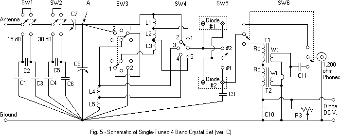
Wiring the crystal radio set: The stator and rotor terminals of C8 are labeled points A and B (see Fig. 5), and all connections to them should be short and direct. The purpose is to minimize spurious FM and short-wave resonances which might be created otherwise. This approach eliminates as much wiring inductance associated with C8 as possible, maximizing its ability to shunt out any high frequency spurious responses that might be present. Some more info on this subject is presented near the end of part 8.
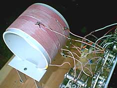
The 'contra wound' tank inductor:
L1, L2, L3 L4 and L5 are all components of the tank. It is wound with litz wire having 660 strands of #46 conductor. L1 has 13 turns, L2 has 3.125 and L3 has 8.875, all close wound (because the form is not long enough to enable spacing and the extra turns that would be required to maintain the inductance) as component inductor #L(1,2,3) with two taps. L4 has 7.25 turns and L5 has 17.75, both close wound as component inductor #L(4,5) with one tap.
The start of L1 of component inductor #L(1,2,3) is spaced 0.06" to the right of the center of the coil form, looking at the crystal radio set from the front and winding continues through L2 and L3 clockwise to about 0.25" of the right end of the form, looking at the crystal radio set from the right. The start of L4 of component inductor #L(4,5) is spaced 0.06" to the left of the center of the form, looking at the crystal radio set from the front and winding continues through L5 clockwise to about 0.25" of the left end of the form, looking at the crystal radio set from the right. When one looks at a completed contra wound inductor, one can see that the component inductors #L(1,2,3) and #L(4,5) are wound in opposite directions. Note: All coil dimensions are measured from turn center to turn center. See Article #0, Part 12 for a mini-Article about the purpose and use of the 'contra wound' inductor. Figures 2 and 3 in Article #29 provide more info on the contra wound inductor approach.
Here is the reason for this winding scheme: One can see from Fig. 4 that this crystal radio set design connects component inductors #L(1,2,3) and #L(4,5) in series for the lower half of the BC band and in parallel for the upper half. If the two coils were wound in the same direction from the hot to the cold end, as was done in the crystal radio set described in Article #22, distributed capacitance would be low in the series connection (about 7.7 pF) and higher in the parallel connection (about 21 pF), mainly because the finish (ground end) of component inductor #L(1,2,3) is located close to the start (hot end) of component inductor #L(4,5). This reduces the Q at the high end of the BC band. If the coils are contra wound, as I call it, the lower distributed capacitance condition occurs in the parallel, not the series connection, resulting a Q increase of approximately 17% at 943 kHz. It is increased even more at the high end of the BC band. The coil form is made of high-impact styrene. OD=4.5", ID=4.22" and length=3.625". I used part #S40140 purchased from the Genova Products factory retail store. (http://genovaproducts.com/factory.htm). A PVC form can be used, but its dielectric has about 4-5 times the loss of the styrene form and will reduce Q, especially at the high end of the BC band.
The start (hot) ends of L1 and L4 are affixed to the form by being lead through two 0.25" diameter holes placed 0.5" apart, measured in the circumferential direction, and held in place by 0.5" wide film tape on the inside of the form. The finish (cold) ends of L3 and L5 are affixed to the form by being lead through two 0.125" holes placed 0.5" apart, measured in the circumferential direction, and held in place as above. Three 0.125" diameter holes spaced 0.5" apart are used when pulling a tap. In Fig. 6, the red line represents the litz wire and the yellow arcs represent a cross-section of the coil form through the center of the 0.125 or 0.25" holes.
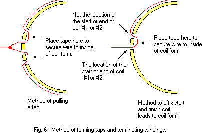
Fig.7 Coil mounting hardware.
To wind the tank coil, first cut five pieces of 660/46 litz as follows: For L1: 16' 9", L2: 4' 3", L3: 11' 10", L4: 9' 11" and L5: 22' 5". These lengths provide about 9" of free length at each end. The ends of each wire length should be tinned to prevent unraveling of the strands and serving while winding the coils. Use a small Weller WC-100 adjustable temperature iron (or equivalent), set to maximum temperature (really hot!) for tinning. The method is to immobilize an end of the wire end by extending it about 2" over the end of a table and placing a weight on top of it. One can then apply the very hot iron tip to the cut strand ends and feed in a little solder to wet them. As the heat percolates down the litz and the insulation burns off or melts, more solder can be applied a little further down and around the end to obtain a solid tinning for a lead length of about 0.25". If one don't want an inch or so of litz beyond the solder to become stiffened from melted insulation, one might do as John Davidson has suggested. He tightly wraps a length of aluminum foil around the litz, up to 0.375" from the end before soldering to act as a heat sink and keep the insulation cool. I haven't tried this out.
The start leads of L1 and L4 should be spaced 0.06", right and left from the longitudinal center of the coil form. One can use a bent up plastic soda straw in the 0.25" holes to keep the wires approximately in place). Gradually taper the wires further apart going through the first turn, then to become close wound for the remainder of the windings.
Table 1 - Longitudinal locations for the taps and start/finish of L1, L2. L3, L4 and L5.
|
Coil name |
Start - inches to right or left of center |
Finish - inches to right or left of center |
| L1 |
0.058 R |
0.81 R |
|
L2 |
0.81 R |
0.99 R |
|
L3 |
0.99 R |
1.50 R |
|
L4 |
0.058 L |
0.48 L |
|
L5 |
0.48 L |
1.50 L |
After the windings are completed, one should have a coil with ten droopy wires coming from it. The next step is to tidy up the coils, adjust the 0.12" wire spacing at the start of L1 and L4 and their one-turn taper. Move any excess winding space to slightly space-wind the last several turns of L3 and L5 at their finishes (cold ends). The turns should then be sprayed with one light application of crystal clear "Krylon" acrylic lacquer, Rust-Oleum Specialty high luster lacquer coating (clear) or equivalent, to hold them in place. The ends of L1 through L5 that are to be joined to form the taps should be cut to a length of about 0.5", tinned and soldered together as shown in Fig. 6. Pigtails for wiring to the switches should now be soldered to the taps. The coil form should be mounted with its axis parallel to the front panel as shown in Fig.1, its center about 6.50" back, and centered horizontally.
Tank coil specs. for those who wish to use a different diameter coil form, axial length of total winding, wire size or wire to wire spacing:
- The total tank inductance, measured from point A to ground, should be 250 uH with SW3 in position 1 and 62.5 uH in position 2. Optimum partitioning of turns: L1 should comprise 26.1% of the sum of the turns of L1, L2, L3, L4, and L5; L2: 6.15%; L3: 17.75%; L4: 14.5% and L5: 35.5%. To get the highest Q in sub-bands 3 and 4 it is essential that the sum of the turns of L1, L2 and L3 equals the sum of the turns of L4 and L5. The values for L1 and L2 are compromises when SW3 is set to position 2 (normal selectivity on sub-bands 1 and 3). They minimize the error caused by using the same number of turns to ground at that setting. See Table 2.
- It is desirable that the start and finish ends of the coils on the form (as mounted) should be located on that half of the coil form nearest the front panel. This will prevent taps from being located on the far side of the coil, as viewed from the front panel, thus preventing excessive lead lengths.
- Some experimentation in tradeoffs of the requirements in 1.) and 2.) may have to be made, since they may not be fully compatible.
The diode: This design is optimized for use with a diode having an n of 1.03 and a Saturation Current (Is) of about 106 nA at 25° C., although this is not critical and other diodes can be used with very good results. See Articles #0, 4 and 16 for info on n and Is of diodes, and how to measure them. If one has a favorite diode, its effective (Is) can be changed by applying a DC bias voltage, using perhaps, the 'Diode Bias Box' described in Article #9.
An excellent diode to use in this set is the ITT FO-215 germanium unit that was made 20 or so years ago (see Article #27). NOS may be available from from Dave Schmarder at http://www.1n34a.com/catalog/index.htm and Mike Pebble at http://www.peeblesoriginals.com
Another suitable diode, the published parameters for which show an (Is) of 100 nA is a Schottky diode, the Agilent HBAT-5400. It is a surface-mount unit that was originally designed for transient suppression purposes. Measurements of many HBAT5400 diodes seem to show that there are two varieties. One type measures approximately: n=1.03 and (Is)=80 nA The other type seems to have an n of about 1.16 and an (Is) of about 150 nA Both work well but the former works best. This part, available in an SOT-23 package is easily connected into a circuit when soldered onto a "Surfboard" such as manufactured by Capital Advanced Technologies (http://www.capitaladvanced.com/), distributed by Alltronics, Digi-Key and others. Surfboard #6103 is suitable. The HBAT5400 is also available in the tiny SO-323 package that can be soldered to a 330003 Surfboard.
The Agilent HSMS-2860 microwave diode (Specified Is=50 nA) is available as a single or triple with three independent diodes in the SO-323 and SO-363 packages, respectively. The Agilent number for the triple diode is HSMS-286L. I find it to be particularly good for DX in this crystal radio set. It is a convenient part since one can connect it using only one section (shorting the unused ones) or with two or all three in parallel. This gives one a choice of nominal saturation currents of 50, 100 or 150 nA Samples of this part I have tested measured about 35 nA per diode, not 50. I don't know the normal production variations. The only disadvantage of this diode, as far as I know, is its low reverse breakdown voltage which may cause distortion and low volume on very loud stations. It has the advantage, as do most Schottkys, of having much less excess reverse leakage current than do germanium diodes. This helps with volume and selectivity on very weak stations.
Infineon makes a BAT62 Schottky diode in several different small surface mount packages. The single BAT62 is physically the largest and easiest to handle. It has a specified (Is) of about 100 nA and performs quite well.
Most germanium diodes have too high a saturation current for the best selectivity when receiving weak signals and should to be back-biased or cooled for optimum performance, although the difference is usually hard to notice. See Article #17A for more info on this.
Different type diodes may be connected to the terminals labeled Diode #1 and Diode #2, with either one selectable with SW5. When one diode is selected, the other is shorted. This feature makes it easy to compare the performance of a 'test' diode with one's 'favorite' diode. Another use is to place one's best DX diode in one position and one having a very low reverse leakage current at high reverse voltages in the other. This will maximize volume and minimize audio distortion on strong signals.
A good choice for this crystal radio set is a diode having a relatively low saturation current such as 3 or 4 Agilent HSMS-2820 or HSMS-2860 diodes in parallel as Diode #1 for high selectivity and sensitivity on weak signals, and an Agilent HBAT5400 or one of the lower saturation current germaniums as Diode #2 for low distortion and maximum volume on very strong stations. Don't use two diodes in series if you want the best weak signal sensitivity in any crystal radio set. The result of using two identical diodes in series is the simulation of an equivalent single diode having the same (Is) but an n of twice that of either one. This reduces weak signal sensitivity.
Different type diodes may be connected to the terminals labeled Diode #1 and Diode #2, with either one selectable with SW5. When one diode is selected, the other is shorted. This feature makes it easy to compare the performance of a 'test' diode with one's 'favorite' diode. Another use is to place one's best DX diode in one position and one having a very low reverse leakage resistance at high reverse voltages in the other. This will maximize strong signal volume and minimize audio distortion.
Audio impedance transformation: from the audio output resistance of the diode detector to 'series connected' 1.2k ohm sound-powered phones is provided by the audio transformers. If one wishes to use 300 ohm sound-powered phones with two 600 ohm elements connected in parallel instead of series, a very good low loss transformer choice is the 100k-100 ohm transformer from Fair Radio Sales, #T3/AM20. The configuration of two Calrad transformers shown on line 2 of the Calrad chart in Article #5 is also a good choice. C11, along with the shunt inductance of the transformer and the inductance of the sound powered phones form a high-pass filter, flat (hopefully) down to to 300 Hz. R3 is used to adjust the DC resistance of the diode load to the AC impedance of the transformed effective AC headphone impedance to minimize audio distortion on very strong signals. C10 is an audio bypass.
The two variable capacitors C7 and C8: interact substantially when tuning a station. C7 mainly controls the selectivity and C7 and C8 together control the resonant frequency. Reducing the capacitance of C7 increases selectivity. If the antenna-ground system has a resistance larger than 25 ohms, C7 will have to be set to a smaller capacitance in order to maintain the proper resonant resistance at point A in Fig. 5. If the capacitance of the antenna-ground system is greater than 200 pF, C7 will also have to be set to a lower value than if it were 200 pF. If the maximum capacitance of the capacitor used for C7 used is not large enough to enable a large enough bandwidth at the low end of sub-band 1, provision can be made to switch a 330 pF NPO ceramic cap in parallel with it. This may be needed if the antenna-ground system has too low a capacitance (small antenna).
The "capacitive" attenuators controlled by SW1 and SW2: Used for volume and selectivity control and are are designed so as to cause minimal tank circuit detuning when the equivalent circuit of the antenna-ground system has the same values as the old IRE simplified Dummy Antenna recommended for testing Broadcast Band radio receivers. It consists of a series combination of a 200 pF cap, 20 uH inductor and a 25 ohm resistance. The geometric mean of the sum of the reactances of the capacitor and inductor at 520 and 1710 kHz is -605 ohms. This is the reactance of a 279 pF capacitor (characteristic capacitance of the "capacitive" attenuator) at 943 kHz, the geometric mean of the BC band of 520-1710 kHz. The "capacitive" attenuators were designed for the specified attenuation values (15 and 30 dB) utilizing the 500 ohm resistive pi attenuator component values table shown in the book "Reference Data for Radio Engineers". The resistor values for 15 and 30 dB "capacitive" attenuators were normalized to 605 ohms, then the "capacitive" attenuator capacitor values were calculated to have a reactance, at 943 kHz, equal to the value of the corresponding "capacitive" attenuator shunt or series resistance. Since the "capacitive" attenuators, when switched into the circuit, isolate the antenna-ground system resistance from the tank circuit, selectivity is increased. If the series capacitance of the equivalent circuit of one's own antenna-ground system is 200 pF, at 943 kHz, practically no retuning is required.
If the equivalent L and C of one's own antenna-ground system differ substantially from those of the simplified IRE dummy antenna used in this design, one can normalize the values of the capacitors used in the "capacitive" attenuators to match one's own antenna-ground system. A method for measuring the parameters of an antenna-ground system is shown in Article #20.
Table 2 - Switch Functions for Version C
|
SW1
|
15 dB volume control "capacitive" attenuator.
'Down' places about 15 dB loss in the input.
|
|
SW2
|
30 dB volume control "capacitive" attenuator.
"Down' places about 30 dB loss in the input.
|
|
SW3
|
520-943 kHz - Band A (sub-bands #1 and #2) - position
1
943-1710 kHz - Band B (sub-bands #3 and #4) - position 2 |
|
SW4
|
520-700 kHz - Band A, sub-band 1. Normal selectivity:
position 2, Sharp selectivity: position 3
700-943 kHz - Band A, sub-band 2. Normal selectivity: position 5, Sharp selectivity: position 4 943-1270 kHz - Band B, sub-band 3. Normal selectivity: position 2, Sharp selectivity: position 1 1270-1710 kHz - Band B, sub-band 4. Normal selectivity: position 4, Sharp selectivity: position 5 |
|
SW5
|
Used to select diode 1 or diode 2.
|
|
SW6
|
'Down' position for normal operation using 1.2k
ohm phones. 'Up' position to bypass the onboard audio transformers
if one wishes to use an external transformer to match an impedance
other than 1.2k ohms.
|
4. Tuning the Crystal Radio Set to to a specific frequency.
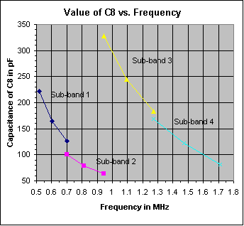
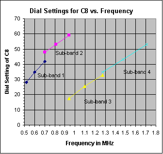
C8 is considered the primary tuning control. C7 is used, in conjunction with the capacity of the antenna-ground system to adjust selectivity to the designed value. It also has considerable interaction with the tuning frequency. There are two methods for tuning in a station of a known frequency that will result in the selectivity being fairly close to specification, as shown in table 5. One requires a knowledge of the capacitance of C8 vs. its dial setting. The second requires fitting C8 with a knob having a linear calibration of 0-100 over a 180 degree span and having a dial reading of zero at maximum capacity. To use this method C8 must be as specified in the parts list or an exact equivalent.
- To tune to a specific frequency, read the necessary capacity for C8
from Fig. 8 and set C8 to that value. Adjust C7 to tune in the
station.
-or-
- To tune to a specific frequency, read the necessary dial setting for C8 from Fig. 9 and set C8 to that value. Adjust C7 to tune in the station.
It is assumed that the tank inductor has the required 250 and 62.5 uH inductance values and is contra wound as described. Of course different inductance values can be used to make a good crystal radio set, but the graphs in Figs. 8 and 9 would have to be changed. It is also assumed, when using the figs. 8 or 9, that the impedance of the antenna-ground system being used is equal to that of the Standard Dummy Antenna.
 |
 |
|
Fig. 8 - Designed capacitance
of C8 vs. Frequency
|
Fig. 9 - Dial setting of C8
when using the specific variable
capacitor specified in the Parts List. |
Another method of tuning is to estimate from Table 3 the dial settings for C7 and C8 required to tune to the desired station. C7 and C8 can then be tuned together higher or lower to actually tune in the station. If more selectivity is desired, reduce the capacitance of C7 and retune C8. If the volume is too low, try increasing C7 and decreasing C8.
|
Dial settings-->
|
0
|
10
|
20
|
30
|
40
|
50
|
60
|
70
|
80
|
90
|
100
|
|
Sub-band 1 switch setup, normal selectivity
|
386
|
423
|
482
|
560
|
650
|
776
|
867
|
994
|
1176
|
1394
|
1606
|
|
Sub-band 2 switch setup, normal selectivity
|
387
|
424
|
484
|
562
|
658
|
765
|
881
|
1015
|
1171
|
1389
|
1581
|
|
Sub-band 3 switch setup, normal selectivity
|
765
|
835
|
951
|
1096
|
1268
|
1466
|
1681
|
1921
|
2192
|
2565
|
2881
|
|
Sub-band 4 switch setup, normal selectivity
|
773
|
839
|
950
|
1104
|
1278
|
1485
|
1708
|
1953
|
2241
|
2650
|
2987
|
5. How to improve selectivity with
a relatively small loss in sensitivity, in addition
to using the "Sharp Selectivity" switch positions on SW 4.
-
Selectivity can always be increased by reducing the value of C7 and retuning C8. If neither "capacitive" attenuator is in-circuit, switching one into the circuit will increase selectivity.
- Selectivity can be increased by changing to a diode having a lower Is than the HBAT5400, such as the Agilent 5082-2835 or HSMS-2820. A DC bias, applied to the 'Diode Bias' terminals can 'fine-tune' performance. The diode 'Bias Box' described in Article #9 is useful here. One can choose less audio distortion and less selectivity by biasing the diode in a more forward direction, or better selectivity, at the cost of more audio distortion by biasing the diode toward its reverse direction.
- Experimentation using a position on SW4 that taps the diode further down on the tank than specified in Table 2.
6. 'Loop Effect' of the tank inductor,
and how it can be used to tame
local 'Blowtorch' stations when searching for DX.
One can use local signal pickup by the tank (loop effect) to reduce the effect of interference from strong stations by rotating the crystal radio set about a vertical axis. The correct angle will generally reduce it.
7. Just how loud is a station that
delivers the amount of power necessary to operate the
Diode Detector at its 'Crossover Point between
Linear and Square Law Operation'?
Many Articles in this series have talked about the 'Linear to Square-Law Crossover' (LSLCP). Please bear in mind that the LSLCP is a point on a graph of DC output power vs input RF power of a diode detector system. It is not a point on a graph of DC current vs voltage of a diode. Two things can be said about a detector when it is fed a signal that operates it at its LSLCP. (1) A moderate increase of signal power will move the detector into its region of substantially linear operation. (2) A similar moderate decrease of input power will move it closer to its region of substantially square law operation where a 1 dB decrease of input power results with a 2 dB decrease of output power.
The crystal radio set described in this Article is operating at its LSLCP if the rectified DC voltage at the 'Diode Bias' terminals is about 51 mV. This assumes a diode having an Is of 106 nA and an ideality factor of 1.03 (such as a selected Agilent HBAT5400 or an Infineon BAT62) is used, with R3 is set to 355k ohms. The audio volume obtained is usually a low to medium, easy-to-listen-to level when using sound power phones.
8. 'Short Wave ghost Signal', 'background hash' and spurious FM reception
All single tuned crystal radio sets may be, in fact, considered double tuned (except single tuned loop receivers). The second response peak arises from resonance between the equivalent inductance of the antenna-ground system and the impedance it sees, in this case, the series combination of capacitors C7 and C8. This peak usually appears at a frequency above the broadcast band and gives rise to the possibility of strong so-called 'short wave ghost' signal interference when a short wave station has a frequency near the peak . The response at this "ghost" frequency can be made somewhat weaker and moved to a higher frequency if the antenna-ground system inductance is reduced. One can use multiple spaced conductors for the ground lead to reduce its inductance. I use a length of TV 300 ohm twin lead, the two wires connected in parallel for this purpose. Large gauge antenna wire, or spaced, paralleled multiple strands helps to reduce the antenna-ground system inductance (flat top antenna). If the down-lead is long compared to the ground lead, use multiple, paralleled, spaced conductors to reduce its inductance (similar to using a 'cage' conductor).
Another possible cause of 'ghost' signal reception resides in the fact that the response of the so-called single tuned circuit does not continuously drop above resonance as frequency rises, but only drops to a relatively flat valley before rising again to the second "ghost" peak. The frequency response above the main (lower) peak would drop monotonically (true single tuned operation) if the second peak did not exist. The relatively flat response valley that exists between the two peaks, provides the possibility (probably likelihood) of interference 'hash' if several strong SW stations picked up at frequencies in the valley range. This also is the cause of a strong local station, above the frequency of a desired station "riding through" and appearing relatively constant even if the tuning dial is moved. The response should drop at a 12 dB per octave rate above the second peak. A useful side effect of the response behavior of this type of circuit is that the response below the main resonance drops off at an extra fast rate of 12 dB per octave rate instead of an expected 6 dB.
The most effective way to substantially eliminate 'short wave ghost' and hash reception is to go to a double-tuned circuit configuration.
Spurious FM reception caused by so-called FM 'slope' detection can occur from close by local FM stations if a spurious FM resonance appears somewhere in the circuitry of a crystal radio set. If ground wiring is not done properly in the crystal radio set, spurious signals can get into the detector. The thing to do here is to run all the RF and audio grounds to one point as shown in Fig.5. Sometimes a small disc bypass capacitor, 22 pF or so, placed across the diode will help.
Another way to try to reduce FM interference is to put a wound ferrite bead 'choke' in series with the antenna and/or ground leads, if the FM interference is coming in on those leads. In order not to affect normal BC band reception, the resultant ferrite inductor should have a reasonable Q and a low inductance in the BC band. It should also exhibit a high series resistance at FM frequencies. Suitable wound ferrite chokes (bead on a lead) are made by the Fair-Rite Corp. as well as others. Two types available from Mouser are #623-29441666671 and #623-2961666671. This suggestion may also help reduce "short wave ghost" signal reception in some cases.
Note: See "Wiring the crystal radio set:", in Part 3, above.
9. Measurements.
|
center of sub-band 1, normal selectivity, using the simplified IRE dummy antenna. |
center of sub-band 4, normal selectivity, using the simplified IRE dummy antenna. |
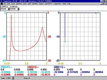
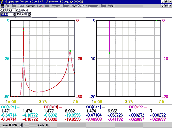
Fig. 10 shows the simulated frequency response at the center of sub-band 1, from the antenna source to the RF input of the diode. The red graph and figures in the left panel show an insertion power loss of 2.4 dB with a -3 dB bandwidth of 6 kHz, along with the spurious response peak at 4.4 MHz, caused by the antenna-ground system inductance. The insertion loss at the spurious peak is 15 dB. The loss in the valley is 40 dB. The right graph and figures show the Input Return Loss (impedance match) at resonance to be -12.2 dB. The output return loss (not shown) is the same.
Fig. 11 shows the simulated frequency response at the center of sub-band 4, from the antenna-ground system source to the RF input of the diode. The red graph and figures in the left panel show an insertion power loss of 4.1 dB with a -3 dB bandwidth of 6 kHz, along with the spurious response peak at 6.9 MHz, caused by the antenna-ground system inductance. The insertion loss at the spurious peak is 20 dB. The loss in the valley is 47 dB. The right graph and figures show the Input Return Loss (impedance match) at resonance to be -8.5 dB. The output return loss is the same.
Fig. 10 and Fig.11 are actually simulations of the RF frequency response of version 'b' as described in Article #22. The response curves of version 'c', described in this article should be the same, with the exception of halving less loss at the peak response points. This is because of the higher tank Q in version 'c'.
Table 4 - Measured unloaded tank Q values. Antenna and diode disconnected, SW1 and SW2 set to -15 and -30 dB and C7 set to 50 on the dial |
||||
|
Band-->
|
Sub-band 1
|
Sub-band 2
|
Sub-band 3
|
Sub-band 4
|
| Frequency in kHz.--> |
520
|
943
|
943
|
1710
|
| Measured unloaded tank circuit Q (includes loss in the tuning caps, switches and all other misc. loss)--> |
1020 |
1000 |
1240 |
940 |
Table 5 - Measured RF bandwidth and power loss @ resonance, at approx. the LSLCP. Diode parameters: Is=106 nA, n=1.03. Output power=15.8 nW=-78 dBW |
||||
|
Center |
Insertion loss in dB, |
-3 dB bandwidth in
kHz, normal selectivity |
Insertion loss in dB, |
-3 dB bandwidth in
kHz, sharp selectivity |
|
603
|
6.5
|
6.3
|
9.0
|
1.9 |
|
813
|
7.3
|
5.0 |
10.0
|
2.2
|
|
1094 |
7.5 |
4.7 |
12.0 |
2.2 |
|
1474 |
8.8 |
5.8 |
13.5 |
2.9 |
The data in Table 5 show the insertion power loss when the crystal radio set is driven by a CW RF signal, with the diode feeding a resistive load of 355k. R3 is used for the resistive load and is set to 355k (be sure to disconnect any diode connected to the terminals when setting R3 for 355k). SW6 is set to the 'down' position. For greatest measurement accuracy, one should short out the series connected primaries of T1 and T2. The signal generator used in the measurements is adapted to have a source impedance equal to that of the standard IRE simplified dummy load (see Article #11). The expected diode detector power loss, at the output power level used, is about 5 dB. The remainder of the insertion loss shown in Table 5 is caused by losses in the inductive and capacitive parts of the tank. Weaker signals will result in a higher detector power loss, stronger signals, a lower loss. Some more info on detector power loss and LSLCP is given in Fig. 2 and its succeeding paragraph in Article #15a.
The signal level used was chosen to operate an HBAT5400 diode having an Is of 106 nA and an n of 1.03 near its LSLCP. The input RF voltage was set to cause a DC output voltage of 0.075 volts* across the R3=355k ohms (measured at the 'Diode DC V.' terminals). This gives an output power of -78 dBW. The signal generator output was varied, depending on the insertion power loss of the passive components as measurements were made at the different frequencies. In practice, one should add about 1.0-2.0 dB to the insertion power loss shown in Table #5 to allow for a typical audio transformer loss. In actual practice, of course, one uses an audio load (headphones), fed through the audio transformer, instead of a resistor for the diode load.
*A diode detector is operating at its LSLCP when its DC load resistance is R=n*0.0257/Is and the detected DC across it is 0.051 volts.
This CW method of measuring loss is much easier than the more complicated
general method using AM modulation, as shown in Article #11.
10. A method for measuring the unloaded Q of an L/C resonator
- Connect the 50-ohm output of a precision frequency calibrated RF generator (I used an Agilent digitally synthesized unit.) to a radiating test loop by means of, say, a 5 foot long coax cable. The loop can be made from 15 turns of solid #22 ga. vinyl insulated wire, bunched up into a ¼" diameter cross section bundle, wound on a 2" diameter vitamin pill bottle. The coil is held together by several twist-ties.
- Make sure that all resistive loads are disconnected from the tank. Remove all potentially lossy non-metallic and metallic (especially ferrous) material from the vicinity of the coil. Capacitively couple the probe of a 5 MHz (or greater) scope to the hot end of the L/C tank and set the probe to its 1:1, not its 10:1 setting. This coupling must be very weak. This can be done by clipping the scope probe onto the insulation of a wire connected to the hot end of the coil (or a tap) or placing the probe very close to the hot end.
- Place the 2'' loop on-axis with the coil, about 6'' from its cold (grounded) end. Tune the generator to fo MHz and adjust the generator output, scope sensitivity and L/C tuning to obtain, say, a 7 division pattern from fo on the scope. Note the frequency.
- Detune the generator below and then above fo to frequencies (fl and fh) at which the scope vertical deflection is 5 divisions. This closely represents a 3 dB reduction in signal. Record those frequencies. You may encounter some hum and noise pickup problems and will have to respond appropriately to eliminate them. It is usually beneficial to conduct experiments of this type over a spaced, grounded sheet of aluminum placed on top of the workbench.
- Calculate approximate unloaded tank Q. Qa=fo/(fh-fl). Calculate the actual Q by dividing Qa by 1.02 to reflect the fact that 5/7 does not exactly equal SQRT (0.5).
- Try reducing the loop magnetic and probe capacitive coupling, and repeat the measurement and calculation. If the Q comes out about the same, that shows that the 50 output resistance of the generator and the scope probe loading do not significantly load the tank.
- Note: When measuring the Q of an inductor with a Q meter it is common practice to lump all of the losses into the inductor. This includes magnetic losses in the inductor as well as dissipative losses in its distributed capacitance. We generally try to get a grip on tank Q values by measuring the inductor with a Q meter, when one is available. We assume that all the loss that affects the measured Q is magnetic loss. Not so, there is also loss in the dielectric of the distributed capacitance of the inductor. Actually, we are measuring an inductor having a specific Q (at a specific frequency), in parallel with the distributed capacity of the coil. We usually assume that the Q of this distributed capacity is infinite, but it isn't. The dielectric of the coil form material makes up much of the dielectric of the coil's distributed capacity and is the controlling factor in causing different coil Q readings when using coil forms made up of various different materials. This distributed capacity is in parallel with the tuning capacitor and can have an important effect on overall tank Q at the high end of the band because there, it is paralleled with the small, hopefully high Q, capacitance contribution from the variable cap. At lower frequencies, the dielectric material of the coil form becomes less important since its contribution to the distributed capacity is swamped out by the larger capacitance needed from the tuning capacitor in order to tune to the lower frequencies.
11. Important information re: maximizing
unloaded tank Q,
especially at the high end of the band.
Every effort should be made to achieve as high an unloaded tank Q as possible in order to minimize RF loss at the desired -3 dB bandwidth (selectivity), and especially when using narrower bandwidths. Somewhat greater insertion power loss and/or broader selectivity may result if components having a greater dielectric loss than those specified are used. Sensitive areas for loss are:
- Q of the coil. See Table 3 for the Q values realized in the tank circuit.
- Stator insulation material used in the variable caps C7, C8. Very important! Ceramic is best.
- Skin-effect resistive loss in the variable capacitor plates. Silver plated capacitor plates have the least loss, brass or cadmium plated plates cause more loss. Aluminum plates are in-between. Rotor contact resistance can be a problem.
- The type of plastic used in slide switches SW1, 2, and 4.
- Front panel material.
- Coil form material. High impact styrene has less dielectric loss than PVC. Styrene forms are available from Genova Products: http://genovaproducts.com/factory.htm . The forms are listed as drain couplers in their "400" series of products.
- Capacitive coupling from any hot RF point, through the wood base to ground must be minimized because it tends to be lossy and will reduce performance at the high end of band A and band B. The steps I took to reduce these losses are: (1) Mounting C7 to the baseboard using strips of 0.10" thick, 0.5" wide and 1.5" long high-impact styrene as insulators and aluminum angle brackets screwed to the baseboard and (2), wiring these brackets to ground. This electrically isolates the capacitor formed from the lossy dielectric of the wooden baseboard from the rotor of C7. Ceramic stand-off insulators can be adapted, in place of the styrene strips for the job. Another way to mount C7 is to make a mounting plate from a sheet of low loss dielectric material, somewhat larger than C7's footprint, and screw C7 on top of it. Other holes made in the plate can then be used, along with small brackets or standoffs to mount the assembly onto the baseboard. Don't forget to wire the metal mounting pieces screwed to the wood baseboard to ground. These same considerations apply to any metal coil mounting bracket, close to a hot end of the coil, used to mount the coil form to the baseboard. The bracket should be grounded to short out its capacitance through the wood baseboard to ground. The contra wound coil configuration used in this crystal radio set is very helpful here since both outside ends of the coil, in band B are at ground potential.
12. Appendix: Design approach for double and single tuned Benodyne versions, as posted to the Discussion Group Rap 'n Tap (edited).
Ben H. Tongue Posted - 25 February 2005 15:53; The Benodyne approach to a double-tuned crystal radio set is shown in Article #23. The basic circuit is that of a conventional double-tuned circuit operating with equal loaded-Q values for primary and secondary. I decided to use equal values of inductance for the primary and secondary coils for convenience. The reason to use the two varicaps, C7 and C8 (in the primary circuit in unit #1), connected as they were in the crystal radio set in Article #22, is to enable an adjustable impedance transformation (vs. Frequency) between the antenna-ground system source resistance (assumed to be 25 ohms) and the top of the tank (point A). Since the primary and secondary inductors are of the same value and their loaded Q values are designed to be equal, the transformed antenna-ground resistance at the top of the primary tank should be made the same as that at the top of the secondary tank, including loading from the diode. These values are approximately (at band center): LoLo band:250k; HiLo band:500k; LoHi band:500k; HiHi band:1000k. Since the diode RF load is tapped at the 0.707 voltage point for bands HiLo and HiHi, the RF resistance driving the diode is in these cases is 250k and 500k respectively, the same as in the case of the LoLo and HiLo bands. If the diode was not tapped at the 0.707 voltage point for bands HiLo and HiHi, their band-center -3 dB bandwidths would be twice as wide as those of bands LoLo and LoHi. This equalizes all four band-center bandwidths to the desired value. If the tank inductance were the same for the four bands, the -3dB bandwidth at the center of the LoHi and HiHi bands would be four times as great as that at the center of the LoLo and HiLo bands. To correct this condition, the tank inductance in bands LoHi and HiHi is reduced from the 250 uH used in bands LoLo AND HiLo to 62.5 uH. This reduces the -3dB bandwidths at the center of bands LoHi and HiHi so they are the same as the bandwidths at the center of the LoLo and HiLo bands. There is some conflict in the design of a crystal radio set for best performance on strong signals (well above the "Linear-to-square-law crossover point), and one designed for weak signals (well below the "Linear-to-square-law crossover point), when one uses the same diode and audio transformation in both instances. This is because for strong signals, the RF input resistance of the diode detector is about half the audio load resistance, and the audio output resistance of the detector diode is about 2 times the RF source resistance driving it. The conditions for weak signal reception are different. Both the input RF and the output audio resistance of the diode detector are equal to the axis-crossing resistance of the diode. This resistance is Rd=0.026*n/Is (see Article #0 for a discussion on this). The compromise selected was to make the audio load resistance about 325k ohms. The design is optimized for a compromise diode having an Is of about 100 nA and an n of about 1.03. This diode has an axis-crossing resistance of 265k ohms. Most ITT FO-215 diodes have this characteristic. Many others can be used, with little effect on strong signal performance. The diode has more effect on weak than on strong signal performance. A ferrite stick inductor could do well for the coil in the antenna tuner (unit #1) if it has a high enough Q.
Bear in mind that the secondary coil should be constructed with the 250/62.5 uH contra wound arrangement and the 0.707 voltage taps. For this unit, the detector tuner, a 365 pF variable cap would be OK; the extra capacitance of a 485 pF capacitor is not necessary. The inductor for the antenna tuner should be constructed using the contra wound 250/62.5 uH arrangement, but no 0.707 voltage taps are needed.
It is possible to build a double-tuned Benodyne using primary and secondary coils of unequal values. I chose using equal values. A higher inductance for the primary might give some impedance matching problems at the low end of the LoLo band. A lower inductance for the secondary would require a lower RF loading resistance from the diode, thus requiring a diode having a higher Is. Look at Fig. 2 in Article #27 to see how weak signal sensitivity is reduced when using diodes having higher values of Is. For anyone interested in building a single or double-tuned Benodyne, it is suggested that the design be based on version "c" described in this Article, and not version "b", described in Article #22.
#26 Published: 02/10/2003; Revised: 10/23/2006
060610