How to reduce diode detector weak signal insertion-power-loss to less than that possible when the input is impedance matchedBy Ben H. Tongue Quick Summary: Diode detector insertion power loss can be reduced below the value achieved under impedance matched conditions provided it is operating below its LSLC point. The optimal conditions are: (1) The output audio load resistance equals twice the RF source resistance. (2) The Saturation Current and Ideality Factor of the diode are such that the very-low-signal output resistance of the detector (axis-crossing resistance, aka Rd, of the diode) equals the output load resistance. These conditions insure an impedance match at the audio output and a 1:2 mismatch at the RF input (source resistance = half the RF input resistance of the diode). Please bear in mind that the LSLC point is a point on a graph of output DC power vs input RF power of a diode detector system. It is not a point on a graph of DC current vs voltage of a diode. Info on the LSLC point is available in Article #15a. It has usually been assumed by myself and others that power loss in
a two port device (here, a crystal set) is minimized when its input
and output ports are impedance matched. This article will show
that this is not true in the case of a diode detector operating
at a signal power level well below that of its region of essentially
linear operation. It is true, however, when a strong signal
(well above the LSLC point) is being received. In the linear region,
audio output power is proportional to RF input power. That is,
for every dB of change in input power there will be one dB change of
output power. In the lower power region, called the 'square law'
region, a change of one dB in input power results in a two dB change
in output power. See Article #15a, Figs. 2 and 3 for info on the
LSLC point of a diode detector. Definition of terms: Rd: Resistance of a diode at its axis crossing. Rd=0.0257*n/Is at 25 degrees Celsius
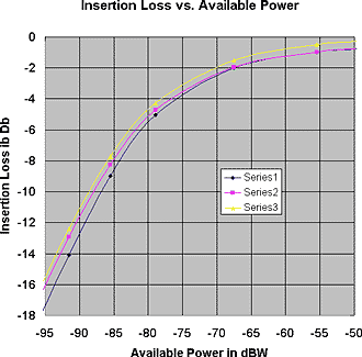
It has been asserted in these Articles that the RF input and audio output resistances, Ri and Ro, of a diode detector, approach the same value and equal 0.0257*n/Is = Rd ohms at room temperature when the input signal strength is low enough. See Article #0, part 4, Article 4, part 2 and Article 16 for information on Is and n, and ways of measuring them. Fig. 1 represents a conventional diode detector. The tank circuit T is shown with no internal loss. A real world tank will have loss that can be represented by a shunt resistor connected across it. For convenience of analysis it is assumed that this loss resistance is absorbed into the source V1, R1 (For a more complete explanation, see Article #1, first paragraph after the third schematic.). Assume that the impedance of the source (antenna) and load (headphone) are transformed to equal values (R1 = R2) and select a diode that has an Rd equal to them. This will result in a reasonable impedance match at both the input and output if the signal power level places operation below +10 dB of the linear-to-square law crossover point. Little of the input power directed towards the detector will be reflected back to the source and most all of the output power from the detector will be absorbed in the load, R2. If the diode detector were a linear device with linear input and output resistances, this impedance-matched condition would result in the least detector power loss (greatest sensitivity) obtainable. It would seem clear that the crystal set detector could not be made more sensitive. Actually, not so! Very weak signal sensitivity can be improved by about 2 dB by appropriate mismatching at the input. This provides a rather hard-to-hear increase in volume, but every little bit helps. In the impedance matched condition discussed so far, R1=Ri=Rd and R2=
Ro. Simple math shows that the detector input voltage Vi will
equal one half the internal source voltage V1. If we create
an impedance mismatch between the source resistance R1 and the detector
input resistance Ri by replacing the diode D with a different one having
1/2 the saturation current, Vi will increase. The reason is that
the detector input resistance Ri is now twice R1. The voltage
divider made up of R1 and Ri will reduce Vi to only two thirds
of V1, making the new value of Vi=4/3 the old value. Since the
detector is operating in square law mode, the internal source voltage
in the detector that drives its output terminals will be (4/3)^2=1.77...
times as much as before. This higher voltage will be divided down by
the voltage divider action of the now twice-as-large diode output resistance
and R2 to give an output voltage 1.185 as large as before. This
equates to an output power 1.476 dB greater than in the original impedance
matched condition.
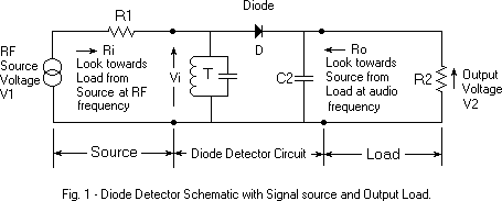
Theoretical calculation and SPICE simulation show that that in a crystal set having equal values for R1 and R2, the diode parameters that give to lowest insertion power loss at low signal power levels fits the equation: R1=R2= 2*(0.0257*n/Is) at room temperature. Now let us look at the effect on Ri and insertion power loss if Ri does not match R1. Look at Fig. 2.
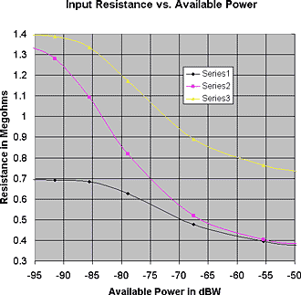
Look at Fig. 3. At the -95 dBW end of the graph, one can see that changing Is from 38 to 19 nA, and keeping R1 and R2 at at 700k ohms reduced the detector insertion power loss by about 1.5 dB (Series 1 to series 2). This comes from the increased voltage, Vi, at the detector input. Raising the output load resistance from 700k to 1400k ohms reduces the mismatch loss at the output to approximate. zero and reduces the overall insertion power loss by another approximate. 0.5 dB for a total improvement of 2.0 dB at low input power levels (Series 3). The detector insertion power loss at the -50 dBW input level is is also reduced by 0.5 dB because of the elimination of the output impedance mismatch. Practically speaking, what does all this mean? Mainly, improved theoretical understanding of diode detectors. (see last bullet point)
#28 Originally published as Article #15 in Feb. 2001; later withdrawn.
Republished as Article #28: 03/04/05 |