A Crystal Radio Diode Detector Simulation using SPICEby Ben H. Tongue
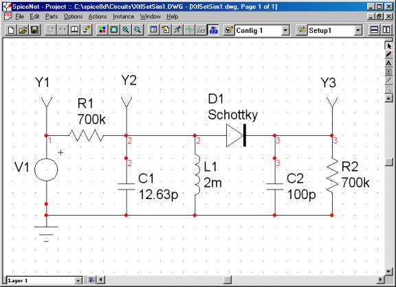
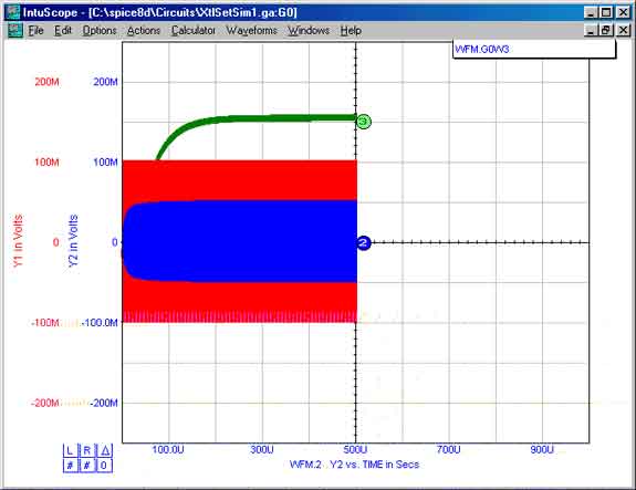
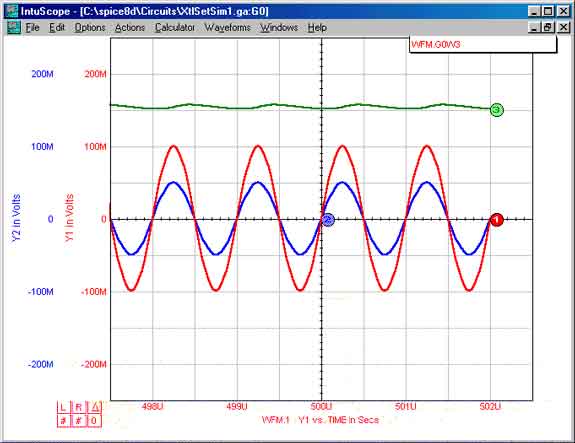
A crystal radio set detector may be simulated in Spice by using a voltage source V1 feeding a parallel tuned circuit L1|C1 through a source resistance R1. The parallel tuned circuit may be made to have any Q by placing a parallel resistor across the tuned circuit. In the simulation circuit files enclosed, an infinite Q is assumed (no RF tuned circuit losses). The actual source loaded Q of the tuned circuit is R1/(Reactance of C1 at resonance). The voltage at the hot end of the tuned circuit is connected through a diode D1 to a parallel RC load R2|C2. The detected output voltage is developed across this load. The purpose of doing this is to enable experimentation to determine how the detection sensitivity changes if the diode type, diode source resistance, and/or load resistance are changed. This program enabled me to develop the graphs shown in Article #1 on my home page that show how detector power loss varies as a function of rectified diode current for a HP 5082-2835 diode and also, more importantly, as a function of diode saturation current Is. The input voltage is modeled as an un-modulated 1.0 MHz sine wave consisting of 4002 individual cycles, sampled at eight points per cycle. If one wants to evaluate the result of using an AM modulated wave, three simulations can be made using min., carrier, and max. Voltage levels of the desired modulated wave. Note: Graphs of diode current and voltage waveshapes, as a function of signal power, may be viewed in Article #8. One of the simulations in the enclosed Zip archive 'Crystal Set SPICE Simulations' (click here) uses a Spice model of a Schottky diode similar to the HP 5082-2835. This is called simulation XtlSetSim1 and its files are contained in the directory XtlSetSim1. The other simulation uses a Spice model of the 1N34A. This is called simulation XtlSetSim2 and its files are in the directory called XtlSetSim2. Each of these directories contains all the files that were generated by my SPICE simulator when I ran each simulation. The diodes used in each of these models have the value of CJO set to 0.0 pF. This does not effect the simulation and makes it easier to experiment with various values of C2 without the detuning effect of CJO. The input source and output load resistance values are equal and match the diode RF input impedance and audio output impedance values. One would expect this condition to give the lowest loss (highest Xtal Set sensitivity) at very low signal power levels. This is not so because at very low input power levels, the diode detector exhibits a square law relation, not linear relation between output and input power. See Article #15 for an explanation of how a theoretical 2 dB increase in detector output can be obtained by a deliberate RF mismatch. In XtlSetSim1 the input sine wave voltage is set to a peak value of 0.1 volts. Since the source resistance is set to 700,000 ohms, the power incident on the detector is -57dBm. The output power delivered to R2 is -68dBm at 10.5 mV. The scale is not shown for the green output curves in the graphs below. That scale is 0.002 mV per division with the zero depressed two divisions below the zero centerline used by the other graphs. A broadcast AM voice signal, if it developed a peak instantaneous power in the detector load of -68dBm, would be just sufficient to enable me to understand about one half the words. This assumes that I am using headphones of an equivalent 700,000 Ohms AC impedance having the power sensitivity of a good real world Sound-Powered Headset. (The 700,000 Ohm impedance, of course would be obtained with the aid of an audio transformer.) The RMS audio power would be about 18dB less or -86dBm. Of course, the impedance values used here are quite high, but they are the values I achieve in my loop crystal radio set. To find out where the -18 dB came from, see Article #1, end of part 1, from the home page. In XtlSetSim2 the input sine wave is set to a peak value of 0.045 volts. Since the source resistance is set to 16,000 ohms, the power incident on the detector is -47dBm. The output power delivered to R2 is -68dBm, the same as in the XtlSetSim1 example. The audio load used is 16k ohms. Note that the insertion loss in XtlSetSim1 is 68-57=11 dB. The loss in XtlSetSim2 is 68-47=21 dB. XtlSetSim1 requires 10 dB less input than XtlSetSim2 for the same output! XtlSetSim1 uses a diode with a saturation current Is=40 nA and n=1.08. XtlSetSim2 uses a diode of Is=2600 and n=1.6. The second graph in article #1 on this site predicts that the loss difference would be 8dB. This experiment illustrates that a detector using a of a lower Is, if it is matched at the input and output, will have a lower loss than one using a diode of a higher Is. I have found, since this article was written, that in a 1N34A germanium diode, the values of Is and n change at low currents. Is may go down as much as 5 times and n may drop 25% from the values used in simulation XtlSetSim2. (Those values were obtained at an unrealistically high diode current of about 320 uA.) This was not expected. The result is that the germanium diode is unfortunately shown incorrectly and in a very unfavorable light (for crystal radio set use). The simulation in XtlSetSim2 probably should have used an Is of about 700 nA and n should have been about 1.15. I used the SPICE program from Intusoft called ICAP4WINDOWS demo version. It can be downloaded for free from their Website at http://www.intusoft.com. The netlists: XtlSetSim1.cir and XtlSetSim2.cir can be edited and used in any other SPICE simulator. Keep the following things in mind:
#6 Published: 01/02/00; Last revision: 11/23/01 |