In this article I am going to show an analysis of the operation of a crystal radio set detector using a SPICE simulator. The detector voltage and current waveforms will be shown for three different input "available power" sources. These sources will supply either -85.54, -65.54 or -45.54 dBW (number of dB's below one Watt) power to a matched load. Each power source is made up of a pure voltage source combined with a resistance. (The combo could also be referred to as a "voltage source with an internal resistance"). In each case the available input power, the output power and detector insertion loss will be shown. Conformance to or deviation from the usually assumed peak-detector model will be investigated. The change in input resistance with change in input power will also be examined. Here is a derivation one needs to know in order to understand the rest of this article. The concept of "available power": If one has a voltage source V with an internal resistance R, then the load resistance to which the maximum amount of power (Pa) can be delivered is itself equal to R. Pa will be called the "maximum available power". Any load resistance other than one equal to the source resistance R will absorb less power from the source. This applies whether the voltage is DC or AC (RMS). An equation for power absorbed in a resistance is voltage squared divided by resistance. In the impedance matched condition, because of the 2 to 1 voltage division from the source resistance and load resistance, one-half of the internal voltage V will appear across the load resistance. The actual power absorbed by the load will be, as indicated in the preceding relation: P = ((V/2)^2)/R = (V^2)/(4R). Half of the power delivered to the series combination of the source resistance and the load resistance will be delivered to the load. The other half is dissipated and lost in the source resistance. In the crystal radio set case the input voltage is AC RF voltage. If the input voltage is referred to by its peak value (Vp) as it is in SPICE, instead of by its RMS value, the equation changes. The RMS voltage of a sine wave is equal to the peak value of that wave divided by the square root of 2. Since the power equation squares the voltage, the equation for the "available input power" changes to P = (Vp^2)/(8R). This is the equation that will be used to calculate available input power to the detector, from the source. Here are some definitions, assumptions and explanations:
The Intusoft ISpice netlist shown below is automatically generated by the SpiceNet program after the schematic and parts values are entered into the program. C:\spice8d\Circuits\XSchottky.cir Setup1
Note 1: In regard to the accuracy of the SPICE diode model, some diodes, notably the 1N34A are unusual. The values of Is and n are not constant and do vary with diode current. Measurements made on one 1N34A shows Is and n values of 2.7E-6 and 1.64 at 320 uA which drop to 1.21E-6 and 1.34 at 32 uA, then down to 6.6E-7 and 1.05 at 1.8 uA. Schottky diodes seem to have constant values for n and Is. The SPICE netlist above shows, as the input, a 1.0 MHz sine wave of
peak amplitude 0.125 volts for V1. (This Input signal level is 2.74 dB
less one that would operate the detector half way between the linear and
square law modes. At this lower input signal power level the insertion
power loss of the detector is 7.12 dB). The first of the three simulations
will be done with an input sine wave of 0.125 volts peak for V1 as shown
in the netlist. The second simulation will use a 1.25-volt peak sine
wave. The third will use a 12.5-volt peak sine wave. The respective
available input powers are: -85.54 dBW, -65.54 dBW and -45.54 dBW (dB below
one Watt).
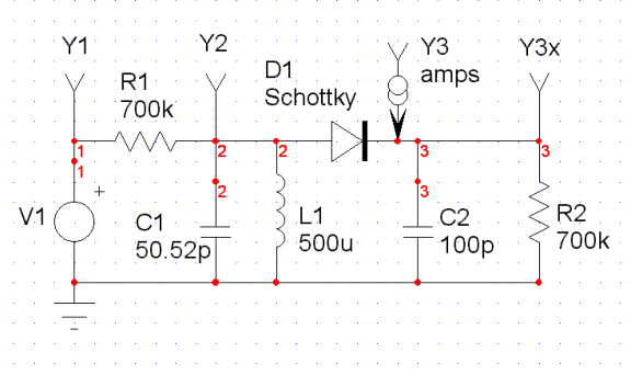
The black curve shows the diode current. The other three curves
all use the same scale on the vertical axis. The blue curve shows
the voltage at the test point Y2. This is the voltage across the
tuned circuit. It has a peak value of 61.9 millivolts, about 1/2
that at test point V1. This shows that the detector has an input
resistance of about 700k Ohms. There is a good input impedance match
here. The red curve shows the voltage across the diode. Note
that where it is positive, a forward diode current flows for about 42%
of the time for one cycle of the 1.0 MHz wave. Note that where it
is negative, a reverse diode current flows. This reverse current flattens
out and if a higher input signal was used, it would flatten out at about
38 nanoAmps, the saturation current of the diode. Finally, note that
there is no peak detection going on. The diode output voltage, measured
at test point Y3x is only 15.7 millivolts even though the peak forward
voltage applied to the detector is 61.9 millivolts. Input power as
stated above is -85.54 dBW. The output power is ((0.0157)^2)/700k = -94.53
dBW. Insertion loss = 94.53 - 85.54 = 8.99 dB.
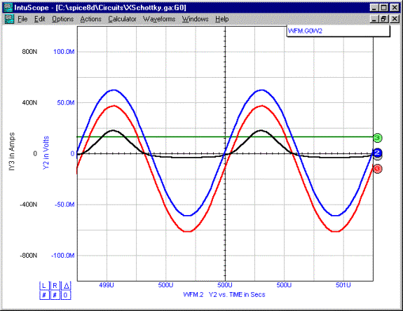
Here, the input voltage at test point Y1 is 1.25 volts, but the voltage
across the LC tank circuit, as measured at test point Y2 is only 494 millivolts,
not 625 which would be the case if we had a perfect impedance match.
This shows that the detector input resistance is now lower than 700k Ohms.
Diode operation is getting closer to peak detection. The green output voltage
at test point Y3x is 361 millivolts. Forward current is now drawn
over about 24% of one cycle time. The input available power, as stated
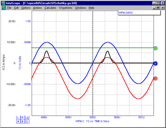
Now it looks as if we are getting much closer to peak detection. The peak positive voltage applied to the diode at test point Y2 is 4.30 volts. The detected DC voltage at test point Y3x is 4.08 volts (only about 5% less than the 4.30 volt peak). The diode forward conducts only during about 12% of the cycle time of the 1.0 MHz wave. As stated before, the input available power is -45.54 dBW. The output power calculates as: ((4.08)^2)/700k = -46.23 dBW. Detector power loss goes down to: 46.23 - 45.54 = 0.69 dB. The input resistance is now even lower than before. The green output voltage at test point Y3x is 4.08 volts, kind of low compared with the 6.25 volts we would get with a perfect input impedance match. Why is this? The input and output resistances of a diode detector both approach the value (0.026*n)/Is Ohms at low signal power levels. (n and Is are diode parameters used in SPICE. n is called the diode Ideality Factor, or Emission Coefficient. Is is called diode saturation current.) Is is defined as the current that is asymptotically approached in the diode back bias direction before extraneous leakage factors or reverse breakdown comes into play. It also has a major effect at an on the amount of current a diode will pass in the forward direction at any specific applied Voltage. As we have seen, as signal input power increases, the quality of the RF impedance match starts to degrade. The AC input resistance to the diode detector decreases from the value obtained in the first well matched low power level simulation. Interestingly, the output resistance increases. The reason for this change is that a new law now governs input and output resistance when a diode detector is operated at a high enough power level to result in a very low power loss. The rule here is that the DC input resistance of an ideal diode peak detector is one-half the value of the output load resistance. Also, the output resistance is equal to two times the value of the input source resistance. Further, since in this example the detector now approaches being a true peak detector, the DC output voltage approaches the square root of 2 times the value of the RMS input voltage. This relationship is necessary in an ideal peak detector so that the AC input power can equal the DC output power with no power lost in the diode (No free lunch). If we were to restore an optimum impedance matched condition by adjusting the input source resistance to 495k ohms and the output load resistance to 990k ohms (by changing the input and output impedance transformation ratios), the power loss would be further reduced to 0.22 dB. See Part 5 of Article #0 for further discussion on the subject of input and output resistance of diode detectors operated in their peak-detection mode. #8 Published: 02/13/00; Last revision: 11/25/01 |